An accurate and predictive model for the infrared dielectric function of a van der Waals material
Future information and communication technologies will rely on the manipulation of not only electrons but also of light at the nanometer-scale. Squeezing light to such a small size has been a major goal in nanophotonics for many years. Particularly strong light squeezing can be achieved with polaritons, quasiparticles resulting from the strong coupling of photons with a dipole-carrying excitation, at infrared frequencies in two-dimensional materials, such as graphene and hexagonal boron nitride. Polaritons can be found in materials consisting of two-dimensional layers bound by weak van der Waals forces, the so-called van der Waals materials. These polaritons can be tuned by electric fields or by adjusting the material thickness, leading to applications including nanolasers, tunable infrared and terahertz detectors, and molecular sensors.
But there is a major problem: even though polaritons can have long lifetimes, they have always been found to propagate along all directions (isotropic) of the material surface, thereby losing energy quite fast, which limits their application potential.
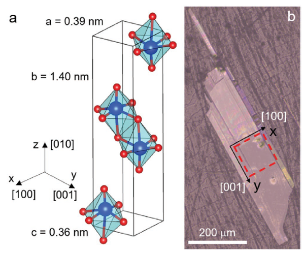
Do anisotropic polaritons exist? Actually, they had been observed experimentally only in artificially structured materials, when two years ago it was reported the first observation of an anisotropic polariton (more precisely, phonon polaritons, the coupling of an infrared photon with an optic phonon) propagation in a natural material: slabs of α-phase molybdenum trioxide (α-MoO3), a van der Waals polar semiconductor . In such materials, an hyperbolic in-plane polariton dispersion leads to an enhanced density of optical states and a ray-like directional propagation along the surface. This discovery placed α-MoO3 at a privileged stage for studying and manipulating light at the nanoscale, beyond what had been achieved with other materials supporting phonon polaritons, such as silicon carbide (SiC) or hexagonal boron nitride (hBN).
Yet, to accurately predict the infrared response of α-MoO3 and thus to enable predictive capabilities for advanced optical devices, it is imperative to develop an accurate dielectric function model. An accurate model would include high- and low-frequency dielectric constants or the phonon damping constants, as these parameters are critical for providing insights into how the crystal lattice dictates the optical response of the material.
Current models using α-MoO3 have relied on a dielectric function that was estimated from reported optic phonon frequencies. This implies assuming the accuracy of these reports of the phonon frequencies, something not granted, and results in an approach that cannot accurately extract the needed constants.
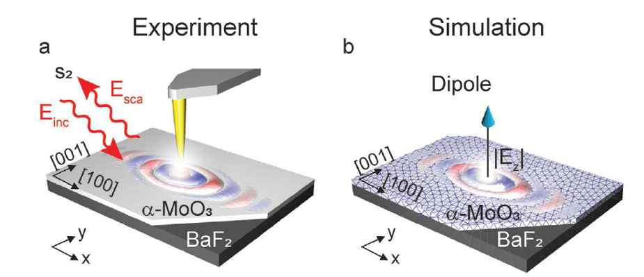
Now, to overcome these limitations, a team of researchers uses 1 a model fitting of polarized far-field infrared spectroscopy on single thick flakes of α-MoO3. This procedure allows identifying the phonon frequencies, high- and low-frequency dielectric constants, and damping rates.
In order to refine this far-field approach and to compensate for any errors induced by the limited lateral scale of the flake, which prevents some measurements, the researchers compared near-field measurements of the damping and the dispersion of phonon polaritons propagating on a thin flake of α-MoO3 to full-wave numerical simulations and calculations that use the initially extracted dielectric function as input. The quantitative agreement between the model and far- and near-field results found was exceptional after an iterative process, dramatically improving the fit and verifying the accuracy and robustness of the resulting dielectric function.
This result not only represents an accurate and predictive model for the infrared dielectric function of α-MoO3, an emerging van der Waals material for nanophotonics. It also offers an innovative approach to extracting dielectric functions of nanomaterials, where the use of traditional methods is challenging or even not possible.
Author: César Tomé López is a science writer and the editor of Mapping Ignorance
Disclaimer: Parts of this article may be copied verbatim or almost verbatim from the referenced research paper.
References
- Gonzalo Álvarez-Pérez, Thomas G. Folland, Ion Errea, Javier Taboada-Gutiérrez, Jiahua Duan, Javier Martín-Sánchez, Ana I. F. Tresguerres-Mata, Joseph R. Matson, Andrei Bylinkin, Mingze He, Weiliang Ma, Qiaoliang Bao, José Ignacio Martín, Joshua D. Caldwell, Alexey Y. Nikitin, and Pablo Alonso-González (2020) Infrared Permittivity of the Biaxial van der Waals Semiconductor α-MoO3 from Near‐ and Far‐Field Correlative Studies Advanced Materials doi: 10.1002/adma.201908176 ↩