A seven-in-one novel instrument for thin film characterization
A seven-in-one novel instrument for thin film characterization
Thin films are defined as material layers ranging from nanometers to several micrometers of thickness that are deposited onto a matrix in order to modify its physical characteristics. Although solar cells conform a relevant field of application, it may be highlighted that the most important employment of thin film technology lies in the semiconductor industry. The constant improvement of wafers as a leading edge technology need from the analytical methods to improve their capabilities in order to obtain a perfect characterization of the product. The complementary metrology, i.e. the use of various techniques to complement each others’ analysis, has been shown to be useful for validate the thickness, material crystal parameters or even the contamination during its manufacture.
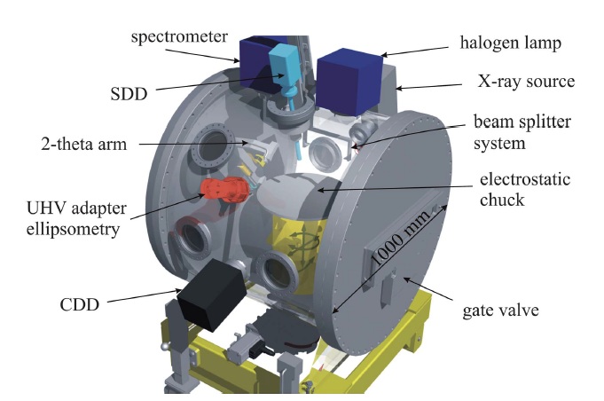
Recently, Holfelder et al. have proposed a platform composed by seven tools for the characterization of 450 mm silicon wafers, which the authors claim would improve the validation of the results while reducing the costs 1. The analytical platform includes an X-ray source (used for 5 different methods based on X-ray fluorescence, reflectrometry, diffractometry and scattering) and a halogen lamp (used for spectroscopic ellipsometry and UV reflectrometry). Several detectors are place all around the chamber to perform the measurements in the same environment. Furthermore, a 5-axis positioning system is included to adjust the sample placement that also enables 2D mapping of the target surface. The angle between the incident radiation and the wafer surface is extremely important for some of the techniques, so in this chamber the exact target placement is ensured. A CAD model of the novel chamber is represented in figure 1.
X-ray fluorescence techniques (XRF) are non-destructive methods based on the radiation of the sample with high energy X-rays and the detection of the subsequent fluorescence emitted from the material. Grazing incidence X-Ray fluorescence (GI-XRF) and total reflection X-ray fluorescence (TXRF) techniques are special cases of XRF, in which the incident angle plays a very important role. The conventional XRF instruments use a fixed angle of incidence, greater than the critical, so the radiation penetrates into the target and the subsequent fluorescence provides the elemental information. It is suitable for quantification and allows high sensitivity analysis, but it is only valid for bulk characterization. Contrary, GI-XRF performs measurement of fluorescence at several incident angles, providing with depth profile measurements of layers even in the nano scale. Furthermore, TXRF systems use an angle of incidence lower than the critical and therefore the radiation is reflected by the sample surface. Thus, the attention is focused at the qualification and quantification of the elemental contamination of the surfaces. The reduction in the scattering of the sample due to its special angle also reduces the background noise, achieving a very high sensitivity. The combination of these techniques allows the elemental characterization of bulk, depth profile and surface contamination components with no need of sample preparation and no material destruction. Thus, an X-ray source with the possibility of variable angles of incidence is included in the analytical platform and SDDs (silicon drift detectors) are used for the fluorescence detection.
The reflection and diffraction of the incidence X-ray are very popular techniques for the characterization of layer thicknesses and crystal structures, respectively. When a sample is radiated by an X-ray beam, part of the radiation is reflected off the surface; however, the reflectivity of that surface may change if another material is deposited on it. X-ray reflectometry (XRR) takes profit of the measurement of the reflected X-ray intensity at different angles, which provides information about the thickness, density and roughness of the thin film deposited on the wafer. On the other hand, XRD (X-ray diffraction) makes use of the scattered beams, which produce diffraction patterns that characterize the crystallographic structure of the material. X-ray diffraction data can not only determine the layer thickness but also the crystal orientation. The analytical platform developed includes the use of diodes as detectors for the reflected beams and the diffraction patterns analysis. The last of the X-ray based techniques present in the chamber is called grazing incidence small angle X-ray scatteringor just GI-SAXS. It makes use of the scattered beams at angles close to the critical of the surface, which allow the measurement of particle sizes in nano structured surfaces. The GI-SAXS technique needs a CCD camera to detect the diffraction pattern. Thanks to these three-of-a-kind techniques it is possible to assure the thickness, roughness and crystallographic orientation of the thin film layers onto the wafer.
Ellipsometry is a technique for the study not only of layer thickness and roughness but also of optical properties, interface quality, band gap and homogeneity. The sample is radiated by a light source (a polarized halogen lamp in the present experiment) using the change of polarization obtained after the reflection. Those changes are characteristic of certain properties of the material. For the analysis of the polarization in the analytical platform under study, it was necessary to couple an analyzer and a photomultiplier to the CCD camera. The light reflected is also analyzed by a spectrometer with a spectral range from ultraviolet to infrared. The optical emission analysis gives information about the layer thickness and material concentration, which conforms the last method, VUV reflectometry.
The recently patented analytical system implements the “seven wonders” techniques for thin films characterization in one compact metrology chamber, while the positioning system aligns the height and tilts the sample depending on the method selected. Thus, it would be possible to perform a total characterization of the 450 mm wafers in an easier, faster and cheaper way.
References
- “Complementary methodologies for thin film characterization in one tool – a novel instrument for 450 mm wafers” I. Holfelder, B. Beckhoff, R. Fliehaug, P. Hönicke, A. Nustch, P. Petrik, G. Roeder and J. Weser. Journal of analytical atomic spectrometry, 2013, 28, 549-557. ↩