A method to calculate elastic quantum transport at the nanoscale
A method to calculate elastic quantum transport at the nanoscale
The field of electronic transport through nanometer-scale systems, such as molecular junctions or atomic wires, has been an extremely active area during the last decades. The effect that the development of a post-silicon era might have on our daily lives, together with the existence of a number of extremely interesting scientific and technological open questions, explain this activity.
The experimental investigation of electron transport across nanosystems was launched with the advent of the scanning tunneling microscope (STM), which enables the measurement of current across a single molecule under the application of an external bias voltage. A few years later, break-junction techniques emerged as alternative ways to measure the transport across molecular bridges. All these techniques have proven to be extremely powerful and, consequently, are still the prime tools for the measurement of transport properties across nanosystems.

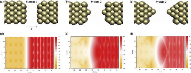
Vvisualized in blue for clarity the left and right primitive unit cells. | Credit: Gracia-Lekue et al (2015)
Along with the huge amount of experimental activity, an equally major effort has been devoted to the development of computational methods appropriate for the theoretical investigation of electron transport at the nanoscale. Due to the difficulty of experimentally probing the detailed atomic structure of the nanosystems, theoretical modeling plays a key role in the understanding and interpretation of experimental observations. After the first semiempirical studies, ab initio simulations based on first-principles have been extensively developed. In particular, given the high sensitivity of conductance to the details of the atomic structure, density functional theory (DFT) has become an essential tool in transport calculations.
Still, DFT methods cannot rigorously handle nanojunctions, open systems that are infinite, nonperiodic and out of equilibrium, because DFT describes systems in their ground state. DFT should be treated, therefore, as a practical method rather than a rigorously exact theory. All in all, in many cases DFT is still the most suitable theoretical tool to study transport properties at the nanoscale.
There are important issues regarding the numerical solutions of the transport problem under the usual DFT formalism. The choice of basis set is of key relevance, being the plane wave the most widely used one in materials science simulation. In a plane wave, the wavefronts are planes. A point source, on the other hand, produces spherical waves, in which the wavefronts are spheres. Recall the simplest and best-known example of interference, Young’s double-slit experiment, in which a monochromatic plane wave is incident on a barrier in which two narrow slits have been cut.
Another important aspect is what is worth trying to calculate. A possibility is to explicitly solve the scattering states. A scattering state can be defined as a wave function satisfying the Schrödinger’s equation at a given energy E, but also satisfying some special open boundary conditions.
Now, Aranzazu Garcia-Lekue and Maia Garcia Vergniory, from DIPC, together with X.W. Jiang (Chinese Academy of Sciences), and L.W. Wang (Lawrence Berkeley National Laboratory) present1 an ab initio method to calculate elastic quantum transport at the nanoscale they have developed during the past ten years.
The method is based on a combination of DFT using a plane wave basis set and auxiliary periodic boundary conditions to obtain the scattering states. The special auxiliary boundary condition is introduced to solve for the ‘‘system states’’ at a given energy E, and these ‘‘system states’’ are linearly combined to obtain the scattering states satisfying the scattering state open boundary conditions. This approach can be applied to any bias voltage.

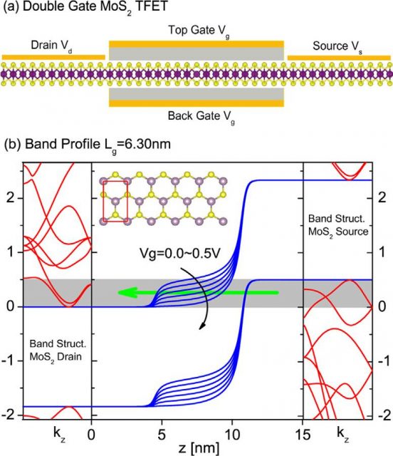
The researchers test their method in different ways: (i) On gold nanojunctions, investigating the tunneling current dependence on the electrode–electrode distance; (ii) describing the surface vacuum states in tunneling through field emission resonances (FERs); (iii) designing a molecular conformational switch based on quantum transport calculations; (iv) and finally, simulating tunnel field-effect transistors (TFETs) based on two-dimensional transition-metal dichalcogenides (TMDCs).

As a result of the tests, the researchers find that: (i) the method is suitable to investigate electron tunneling; (ii) the simulation of the transmission through field emission resonances yields data which can be compared directly with experimental measurements; (iii) the molecule switch can be turned on or off by a perpendicular electric field with known practical limits given by the calculations; and finally (iv) they propose atomic defect designs to further enhance the transistors performance.
All in all, the plane-wave-based transport method provides a good practical and accurate approach to study elastic quantum transport for a variety of problems. And it could be used to study any quantum transport problem, e.g., through transmission from defect states within a semiconductor barrier. Broad applications in the future can be expected.
Author: César Tomé López is a science writer and the editor of Mapping Ignorance.
References
- A. Garcia-Lekue, M.G. Vergniory, X.W. Jiang, L.W. Wang (2015) Ab initio quantum transport calculations using plane waves Progress in Surface Science DOI: 10.1016/j.progsurf.2015.05.002 ↩