A route to the directional control of light–matter interactions at the nanoscale
A route to the directional control of light–matter interactions at the nanoscale

Mobile phones and computers are currently responsible for up to 8% of the electricity use in the world. This figure has been doubling each past decade but nothing prevents it from skyrocketing in the future. Unless we find a way for boosting energy efficiency in information and communications technology, that is. An international team of researchers, including Ikerbasque Research Associate Alexey Nikitin (DIPC), has just published in Nature 1 a breakthrough in quantum physics that could deliver exactly that: electronics and communications technology with ultralow energy consumption.
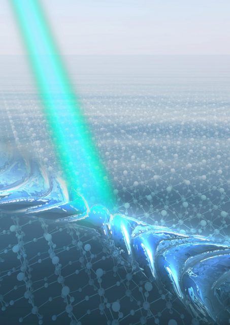
Future information and communication technologies will rely on the manipulation of not only electrons but also of light at the nanometer-scale. Squeezing light to such a small size has been a major goal in nanophotonics for many years. Particularly strong light squeezing can be achieved with polaritons,quasiparticles resulting from the strong coupling of photons with a dipole-carrying excitation, at infrared frequencies in two-dimensional materials, such as graphene and hexagonal boron nitride. Polaritons can be found in materials consisting of two-dimensional layers bound by weak van der Waals forces, the so-called van der Waals materials. These polaritons can be tuned by electric fields or by adjusting the material thickness, leading to applications including nanolasers, tunable infrared and terahertz detectors, and molecular sensors.
But there is a major problem: even though polaritons can have long lifetimes, they have always been found to propagate along all directions (isotropic) of the material surface, thereby losing energy quite fast, which limits their application potential.
Do anisotropic polaritons exist? Actually, they have been observed experimentally only in artificially structured materials. The observation of anisotropic polariton propagation in natural materials has so far remained elusive, though. An this is important since metamaterials are very complex (read expensive) to fabricate. Still, polaritons with anisotropic propagation along the surface of natural van der Waals materials have been predicted. In such materials, an hyperbolic in-plane polariton dispersion would lead to an enhanced density of optical states and a ray-like directional propagation along the surface.

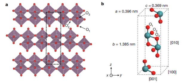
What Nikitin and his colleagues report now is the first images of in-plane elliptic and hyperbolic polaritons (more precisely, phonon polaritons, the coupling of an infrared photon with an optic phonon) that propagate with record-length lifetimes in thin slabs of α-phase molybdenum trioxide (α-MoO3), a natural van der Waals polar semiconductor.

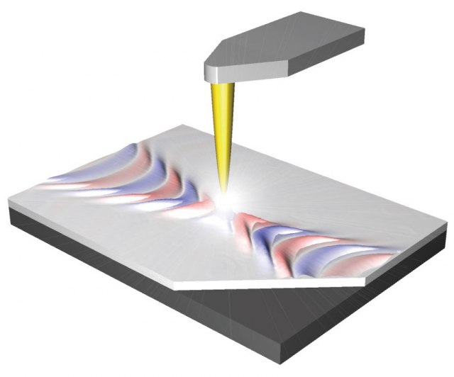
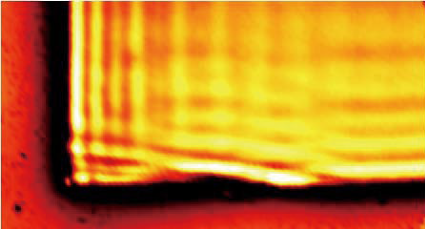
To explore the polaritonic response of α-MoO3, the researchers use a vertically oscillating metallized atomic force microscopy tip illuminated with p-polarized infrared light while scanning an α-MoO3 flake. Acting as an infrared antenna, the tip concentrates the incident field at its very apex to give a nanoscale infrared spot for both the local probing of the material properties and for exciting polaritons (Figure 2). The tip-scattered radiation is recorded simultaneously with topography, yielding nanoscale resolved near-field images. Specifically, the polaritons (described by the field E and wavelength λ) excited by the tip propagate away and are back-reflected at the flake edges, giving rise to interference fringes with a spacing λ/2. (Figure 3).

This way the team visualizes phonon polaritons with elliptic and hyperbolic in-plane dispersion, and with wavelengths (up to 60 times smaller than the corresponding photon wavelengths) comparable to those of graphene plasmon polaritons and boron nitride phonon polaritons. Measurements indicate polariton amplitude lifetimes of 8 picoseconds, which is more than ten times larger than that of graphene plasmon polaritons at room temperature. They are also a factor of about four larger than the best values so far reported for phonon polaritons in isotopically engineered boron nitride and for graphene plasmon polaritons at low temperatures.
These results not only add a new member to the growing list of polaritons in van der Waals materials. In combination with external stimuli, such as strain, electric gating or photo-injection of carriers, it is conceivable that the active tuning of the properties of the anisotropic phonon polariton is within reach. These findings may thus establish a route to the directional control of light and light–matter interactions at the nanoscale.
Author: César Tomé López is a science writer and the editor of Mapping Ignorance.
References
- Weiliang Ma, Pablo Alonso-González, Shaojuan Li, Alexey Y. Nikitin, Jian Yuan, Javier Martín-Sánchez, Javier Taboada-Gutiérrez, Iban Amenabar, Peining Li, Saül Vélez, Christopher Tollan, Zhigao Dai, Yupeng Zhang, Sharath Sriram, Kourosh Kalantar-Zadeh, Shuit-Tong Lee, Rainer Hillenbrand & Qiaoliang Bao (2018) In-plane anisotropic and ultra-low-loss polaritons in a natural van der Waals crystal Nature doi: 10.1038/s41586-018-0618-9 ↩