A photonic crystal the size of a single free space wavelength
A photonic crystal the size of a single free space wavelength

You can read this article because I have used photonics in order to make it possible. It may sound futuristic, but photonics is a technology we use, one way or the other, on a daily basis. Photonic devices are analogous to those used in electronics, but with the electrons replaced by photons. Thus, photonics is concerned with devices involving the transmission, modulation, reflection, refraction, amplification, detection and guidance of light. Therefore, lasers are photonic devices, as the optical fibre that connects me with the world through Internet is.
Closely related with photonics is the field of optoelectronics: those electronic solid-state devices that generate, transmit, modulate or detect electromagnetic radiation, especially at visible, ultraviolet and infrared frequencies. They are most important, because information may travel via an optic fibre but my computer is clearly electron-based. This bring us to the concept of photonic crystal.
A photonic crystal is a material with a periodic nanostructure, in which diffraction of electromagnetic radiation occurs with visible or even infrared light – in ordinary crystals diffraction occurs with X-rays. This means that because the wavelength of visible light is much longer than the wavelength of X-rays the periodicity is much greater in a photonic crystal than in an ordinary crystal.
Thus, photonic crystals offer the possibility to manipulate the flow of light, to enhance light–matter interactions in numerous optoelectronic technologies and quantum optical devices, and to control the spontaneous emission rate of local emitters. At mid-infrared frequencies, photonic crystals find applications as thermal emitters, optical couplers, devices for chemical and biological spectroscopy and sensors for environmental monitoring (e.g., gas sensing).
Photonic crystals are normally fabricated by either patterning silicon slabs or metal layers that are combined with quantum wells (potential wells in which electrons in a three-dimensional system are confined to a plane) operating at the desired wavelength. In both cases, though, there are restrictions to the confinement of light, representing limitations to the dimension of photonic crystals and that of the potential integrated circuits based on them.
One possible way forward are polaritonic crystals. Light confinement can be improved by means of polaritons that, as we know, are modes formed by the coupling of dipolar excitations and electromagnetic fields or, if you prefer, quasiparticles resulting from the strong coupling of photons with a dipole-carrying excitation . Structured thin films of doped semiconductors and graphene supporting plasmon polaritons, or polar dielectrics (such as SiO2, Al2O3 or SiC) supporting phonon polaritons (coupling of an infrared photon with an optic phonon, a phonon being a quantum of vibrational energy), can be seen as polaritonic crystals — lattices with periods comparable to the polariton wavelengths. However, the intrinsic losses of these materials are relatively high, with the exception of SiC slabs but, in this case, fabrication presents substantial practical difficulties.
Promising alternative materials for infrared polaritonic crystals can be found among many low-dimensional van der Waals crystals (materials consisting of two-dimensional layers bound by weak van der Waals forces) that support a diversity of polaritons with unique properties (enormous confinement, tunability, low losses, or negative phase velocity, among others). Particularly, in the mid-infrared frequency range, hexagonal boron nitride (h-BN) crystals exhibit anisotropic phonons and support phonon polaritons. Despite some promising initial works, periodically structured h-BN films in which phonon polaritons can exhibit “collective” modes have not been considered yet, so that until now the concept of a h-BN phonon-polaritonic crystal has remained unexplored.
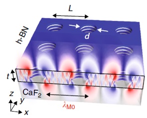
Now, a team of researchers coordinated by the Ikerbasque Research Associate Alexey Nikitin (DIPC) has designed and fabricated 1 a mid-infrared polaritonic crystal formed by a rectangular hole array in a thin h-BN flake. The new photonic crystal is so small, that its whole size is comparable with the wavelength of light in free space (several orders of magnitude smaller than the size of conventional photonic crystals).
The fabrication of the polaritonic crystals started with the obtention of large and homogeneous h-BN flakes. This was achieved through the mechanical exfoliation of commercially available h-BN crystals using a commercial surface protection tape. Afterwards, the flakes attached to the tape were exfoliated and, after inspection with an optical microscope, the large and homogeneous ones were selected. On these, holes were patterned using high-resolution electron beam lithography.
Such crystals support highly confined Bloch modes (the field patterns of a particle in a periodically repeating structure) with flat bands, giving rise to angle- and polarization-independent geometrically tunable resonances, even in case of the simplest square symmetry. Apart of their potential application for subwavelength omnidirectional infrared absorbers, couplers and reflectors, h-BN polaritonic crystals can be utilized for inhibiting spontaneous emission.
Interestingly, the researchers note that the layered structure of the van der Waals material does not play a crucial role in the functionality of the described polaritonic crystal. This means that similar crystals could be potentially obtained with thin layers of isotropic polar or plasmonic materials, where polaritons have low losses. However, the layered structure of van der Waals materials does favor a much easier fabrication of high-quality thin layers via exfoliation.
Author: César Tomé López is a science writer and the editor of Mapping Ignorance
References
- F. J. Alfaro-Mozaz, S. G. Rodrigo, P. Alonso-González, S. Vélez, I. Dolado, F. Casanova, L. E. Hueso, L. Martín-Moreno, R. Hillenbrand & A. Y. Nikitin (2019) Deeply subwavelength phonon-polaritonic crystal made of a van der Waals material Nature Communications doi: 10.1038/s41467-018-07795-6 ↩