How to identify a point defect in 2D transition metal dichalcogenides
How to identify a point defect in 2D transition metal dichalcogenides
A crystal lattice is formed by a repeated arrangement of atoms, ions, or molecules. Due to the enormous amount of atoms involved it is extremely unlikely that all these will be arranged in perfect order. Some atoms will not be exactly in the right place with the result that the lattice will contain defects. The presence of defects within the crystal structure has profound consequences.
Crystal defects are known to modify semiconductor functionality and are expected to have particularly strong impact on the properties of two-dimensional (2D) materials, where screening is reduced compared to bulk systems. In particular, 2D transition metal compounds with two chalcogen atoms (namely, oxygen, sulphur, selenium, tellurium and pollonium), the so-called transition metal dichalcogenides (TMDs), can feature a variety of different defect geometries and related electronic states. Correlating individual structural defects with electronic properties is key for understanding the behavior of and, ultimately, engineering of functional 2D-TMDs. However, the experimental identification of individual defects and the direct correlation of these measurements to their electronic structure is far from simple.
Local crystal defects called point defects appear as either impurity atoms or gaps in the lattice. Impurity atoms can occur in the lattice either at interstitial sites (between atoms in a non-lattice site) or at substitutional sites (replacing an atom in the host lattice). Lattice gaps are called vacancies and arise when an atom is missing from its site in the lattice. Chalcogen vacancies are considered to be the most abundant point defects in 2D-TMD semiconductors, and they are theoretically predicted to introduce deep in-gap states (IGS).
Consequently, important features in the experimental transport characteristic, optical response and catalytic activity of 2D-TMDs have typically been attributed to chalcogen vacancies, based on indirect support from images acquired by transmission electron microscopy (TEM) and scanning tunneling microscopy (STM). Still, there are a variety of technical challenges that limit the direct correlation of TEM studies on TMD materials with their macroscopic response, and the optimization of the material’s performance if based on these results. On the other hand, the strong dependence of the tunneling conditions on the STM contrast of the atomic lattice and the unclear differentiation between chalcogen and metal sublattices in STM studies has led to a non-consistent interpretation of the defect type.
A case in point is the catalytic activity of MoS2. Sulphur vacancies, and their corresponding IGS, have been held responsible for unexpected catalytic activity in hydrogen evolution reactions reported in MoS2. However, this is not consistent with the enhanced catalytic activity reported after long-term ambient exposure of MoS2 samples, since this enhanced catalysis is attributed to oxygen substitution of S atoms, which have been predicted to lack any IGS.
It is apparent that a direct correlation between the atomic and electronic structures of individual defects in 2D-TMDs is required if we want to achieve a fundamental understanding of the effect of defects on the electronic structure.

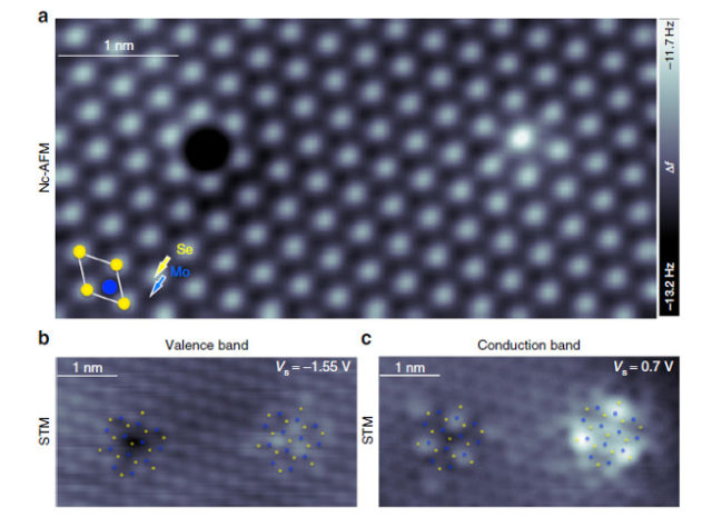
Now, an international team of researchers has taken this bull by the horns 1. They have combined complementary techniques that allow access to the material at the atomic-scale—low-temperature non-contact atomic force microscopy (nc-AFM), STM and scanning tunneling spectroscopy (STS)— together with parallel state-of-the-art first-principles ground- and excited-state calculations using density functional theory (DFT) and many-body perturbation theory within the GW approach, respectively, to enable a comprehensive interrogation of the system. They have been able to demonstrate that the combination of these methods can reveal the structure of the most abundant type of defects in 2D-MoSe2 and 2D-WS2 samples.
The researchers directly relate atomic and electronic structure through combined nc-AFM and STM/STS measurements of individual point defects in monolayer MoSe2 grown by molecular beam epitaxy and in monolayer WS2 grown by chemical vapor deposition. Although nc-AFM and STM images of chalcogen defects appear to be consistent with vacancies, a comparison with DFT and GW calculations establishes these defects as substitutional oxygen at chalcogen sites, consistent with the lack of IGS in the band structure. Therefore, the comprehensive joint experimental and theoretical study reveals substitutional oxygen as a prolific point defect in 2D-TMDs and provides critical insight for future defect engineering in these systems.
Author: César Tomé López is a science writer and the editor of Mapping Ignorance
Disclaimer: Parts of this article may have been copied verbatim or almost verbatim from the referenced research paper.
References
- Sara Barja, Sivan Refaely-Abramson, Bruno Schuler, Diana Y. Qiu, Artem Pulkin, Sebastian Wickenburg, Hyejin Ryu, Miguel M. Ugeda, Christoph Kastl, Christopher Chen, Choongyu Hwang, Adam Schwartzberg, Shaul Aloni, Sung-Kwan Mo, D. Frank Ogletree, Michael F. Crommie, Oleg V. Yazyev, Steven G. Louie, Jeffrey B. Neaton & Alexander Weber-Bargioni (2019) Identifying substitutional oxygen as a prolific point defect in monolayer transition metal dichalcogenides Nature Communications doi: 10.1038/s41467-019-11342-2 ↩