A local quantum emitter can be used to sense the environment of a molecule with the minimal quantum of energy
A local quantum emitter can be used to sense the environment of a molecule with the minimal quantum of energy
Plasmonic nanostructures confine light to dimensions far smaller than the free-space wavelength, as they mix optical fields with electronic excitations. It was not until the 1990s, with the appearance of accurate and reliable nanofabrication techniques, that plasmonics blossomed. It was found then that local fields around nanostructures could be directly measured by near-field scanning optical microscopy. Plasmon nanostructures gained rapid appreciation as routes to optical devices unconstrained by the wavelength of light, yielding viable nanophotonic devices.
A metallic nanoparticle of gold, silver, copper or aluminium exhibits plasmon resonances at wavelengths determined by its material properties, shape and size. For metallic nanoparticles with sharp corners or protrusions, light can be strongly localized to volumes with minimum dimensions of 10–100 nm. Achieving even more tightly confined fields—on the scale of 1 nm or less—is possible but very difficult with single nanoparticles, since there is no fabrication method available offers reproducible control over such small feature sizes.
Fortunately, the large field enhancements associated with nanoparticle clusters can also be achieved with single nanoparticles separated from an suitable substrate by a thin dielectric layer, which behave similarly to a pair or dimer of nanoparticles. This is the case of the gaps between scanning probe tips and metallic surfaces in ultrahigh-vacuum environments.
When a molecule is positioned in the cavity some interesting things happen. For example, recent scanning tunneling microscopy (STM) experiments reported single-molecule fluorescence induced by tunneling currents in the plasmonic nanocavity formed by the STM tip and the substrate. This happens because the electric field of the cavity mode couples with the current-induced charge fluctuations of the molecule, allowing the excitation of photons.
Electronic transport coupled to the field of an electromagnetic cavity can be realized in a wealth of different systems. This includes, besides molecules in plasmonic nanocavities, quantum-dots.
A quantum dot is a nanometric crystalline structure of semiconductor materials. In a quatum dot electrons are confined in a region of space, thus creating a well defined structure of energy levels that depends very much on the size and shape of the quantum dot. This structure resembles that of atoms, that is why sometimes quantum dots are also called artificial atoms.
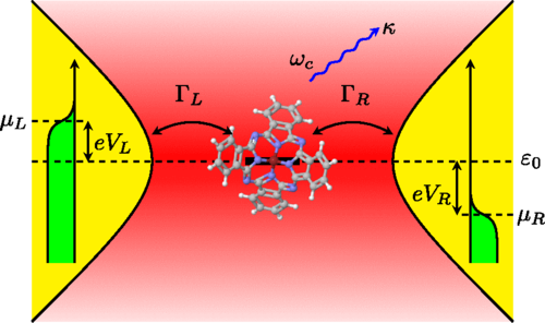
Now, a team of researchers has investigated theoretically such systems 1. The scientists have considered electronic transport through a single-level quantum dot, where the charge on the dot is coupled to the electric field of an electromagnetic cavity. They propose a theoretical model to obtain the current through the quantum dot taking into account the cavity dissipation and arbitrary values of the coupling strength in the incoherent transport regime.
The researchers find that for bias voltages close to the first inelastic threshold of photon emission, the emitted light displays anti-bunching behavior with a vanishing second-order photon correlation function.
The new theory also predicts that strong coupling to a single level allows current-driven non-classical light emission. This prediction can be relevant for a series of experiments on STM cavities.
Finally, and no less interesting, the researchers show that a local quantum emitter can be used to sense the environment of the molecule with the minimal quantum of energy.
Author: César Tomé López is a science writer and the editor of Mapping Ignorance
Disclaimer: Parts of this article are copied verbatim or almost verbatim from the referenced research paper.
References
- Q. Schaeverbeke, R. Avriller, T. Frederiksen, and F. Pistolesi (2019) Single-photon emission mediated by single-electron tunneling in plasmonic nanojunctions Physical Review Letters doi: 10.1103/PhysRevLett.123.246601 ↩