The era of organo-plasmonic devices
One of the greatest inventions of the 20th century, if not the greatest, was the transistor. It revolutionized the electronics industry and changed the way people around the world lived, learned, worked, and played. Its invention marked the beginning of solid state electronics which quickly reduced the size and power requirements of existing electronic tube based electronic devices. This revolutionized the electronics field and eventually made possible the information age thanks to small, low power electronic devices and eventually low cost integrated circuits.
Now, in the 21st century, research is focusing on achieving what the transistor did but using just a few molecules. An these molecules may very well be organic ones: we are entering the era of organic electronics. The emerging devices include organic light-emitting diodes, organic solar cells and organic transistors. But, how can you manufacture and test reliable devices when you have to tune a bunch of molecules, say a couple of hundreds, in a nanometre sized gap? This is not easy at all.
A possible solution may come from hybrid organo-plasmonic devices (HOPD). These devices combine layers of organic molecules with metal nanostructures; as the name indicates, on the surface of these metals coherent delocalized electron quantized oscillations may exist, each of these quanta called a plasmon. The optical characteristics of these HOPD are extremely sensitive to the molecular state, making them suitable for studying the properties of a small number of molecules in a nanogap.
Still there are some issues with this HOPD. A key one is how molecular conductivity influences the optical properties of the plasmonic junction. A group of researchers of the Universities of Cambridge and Leeds, together with Christos Tserkezis and Javier Aizpurua from DIPC and CFM, has now shown1 that an increase in the conductivity of the molecules make plasmons bluer. The results are published in Nano Letters.
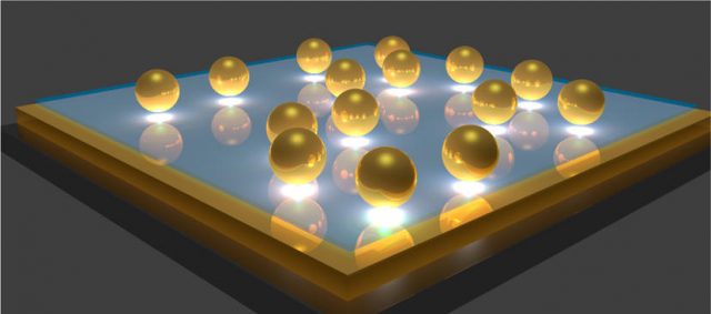
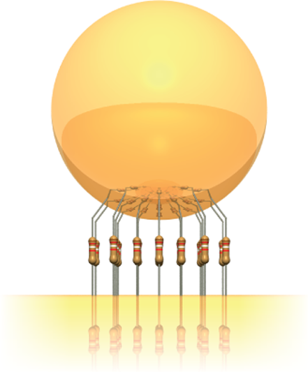
The researchers used a nanoparticle on a mirror geometry. They placed a gold nanoparticle on a gold film coated with a layer of either insulating molecules or conductive ones. This is an easy and reproducible way of assembling HOPD and, furthermore, allows to investigate thousands of identical plasmonic junctions at the same time.
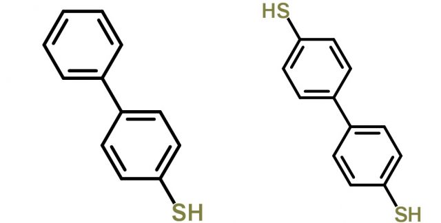
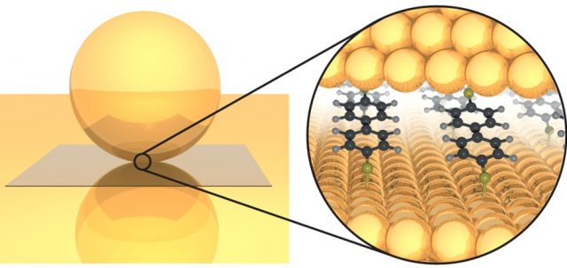
The conductive molecule, 4-4′-biphenyldithiol (BPDT), has two thiol (-SH) groups that form covalent bonds to gold, both in the nanoparticle and in the film, as the groups are located at the ends of the molecule (see figure 3), thus creating a conductive bridge (see figure 4) through the π–cloud of the phenyl rings. The insulating one is very similar, 4-biphenylthiol (BPT), but lacks one of the thiol groups and, therefore, there is no electronic link.
When the molecular layer is changed from the insulating BPT to the conductive BPDT a strong blue-shift of the plasmon resonance can be observed. Samples with layers of mixed compositions of BPT and BPDT were also tested and measurements were made to be sure that the observed effect was not due to the gap size or a change in refractive index. The results, robust and reproducible in thousands of nanoparticles, point to a continuous blue-shift with increasing conductivity.
Electrodynamical simulations confirm that a homogeneous mixed self assembled monolayer exist in the gap between the nanoparticle and the gold film. The simulations also allow to estimate the number of molecules in the gap to be 176 placed in a circle of radius 3.3 nm.
With this result in hand, the resistivity of nanometre sized organic films can be measured optically in a HOPD. The possibility of designing switchable molecules appropriate to this architecture will allow real time electrochemical or optical control of the plasmonic resonance. The field of organo-plasmonic devices is now open.
Author: César Tomé López is a science writer and the editor of Mapping Ignorance.
References
- Benz F., Christos Tserkezis, Lars O. Herrmann, Bart de Nijs, Alan Sanders, Daniel O. Sigle, Laurynas Pukenas, Stephen D. Evans, Javier Aizpurua & Jeremy J. Baumberg (2015). Nanooptics of Molecular-Shunted Plasmonic Nanojunctions, Nano Letters, 15 (1) 669-674. DOI: http://dx.doi.org/10.1021/nl5041786 ↩
2 comments
[…] by yogthos [link] […]
[…] The era of organo-plasmonic devices […]