The extreme nanophotonics of the plasmonic nanopatch
The extreme nanophotonics of the plasmonic nanopatch

For centuries, metals were employed in optical applications only as mirrors and gratings. New vistas opened up in the late 1970s and early 1980s with the discovery of surface-enhanced Raman scattering (SERS) and the use of surface plasmon (collective electronic oscillations at the surface of metals) resonances for sensing.
In a simplified picture and in general, there are five distinctive characteristics that make surface plasmons attractive: their ability to concentrate light beyond the diffraction limit; their ability to modify the local density of photonic states; their ultrafast response; their environmental sensitivity; and their flexibility in design.
Plasmonic nanostructures confine light to dimensions far smaller than the free-space wavelength, as they mix optical fields with electronic excitations. It was not until the 1990s, with the appearance of accurate and reliable nanofabrication techniques, that plasmonics blossomed. It was found then that local fields around nanostructures could be directly measured by near-field scanning optical microscopy. Plasmon nanostructures gained rapid appreciation as routes to optical devices unconstrained by the wavelength of light, yielding viable nanophotonic devices.
A metallic nanoparticle of gold, silver, copper or aluminium exhibits plasmon resonances at wavelengths determined by its material properties, shape and size. For metallic nanoparticles with sharp corners or protrusions, light can be strongly localized to volumes with minimum dimensions of 10–100 nm. Achieving even more tightly confined fields—on the scale of 1 nm or less—is possible but very difficult with single nanoparticles, since the no fabrication method available offers reproducible control over such small feature sizes.
Fortunately, the large field enhancements associated with nanoparticle clusters can also be achieved with single nanoparticles separated from a metal film by a thin dielectric layer, which behave similarly to a pair or dimer of nanoparticles. This is the case of the gaps between scanning probe tips and metallic surfaces in ultrahigh-vacuum environments. These gap modes have complex behaviours and enter the regime of ‘extreme nano-optics’ because they can be sensitive to single-atom placements.
This geometry, which has been known variously as a nanopatch optical antenna, nanoparticle-on-mirror (NpoM), metastructure, metal–insulator–metal (MIM) waveguide, or particle over surface, has become increasingly studied for a wide variety of optical phenomena. The attractiveness of the plasmonic nanopatch or NPoM stems from its ease of fabrication combined with the extreme field enhancements available in either colloidal or lithographically patterned systems.
The plasmonic nanopatch has proven a remarkably successful and robust platform for demonstrating a wide variety of optical phenomena. Jeremy J. Baumberg (University of Cambridge), Javier Aizpurua (CFM & DIPC), Maiken H. Mikkelsen (Duke University) and David R. Smith (Duke University) have now reviewed 1 the physics of the nanopatch, providing intuitive interpretations of its properties and exploring its use across different application areas.
Recent demonstrations that light can be trapped in optical modes of nanogaps with rigorously defined mode volumes below 1 nm3 from surface atoms shows why nanogap plasmons are so important. Every gold surface supports adatoms, but normally the tight confinement into atomic-scale modes leads to negligible interaction with free-space photons. Only due to impedance matching of the plasmonic antennas and nanogaps to free space is it now possible to couple into and out of these highly localized modes with efficiencies beyond 10%. When there are intermediate stages through successively tighter-confined plasmon modes, this coupling can be improved by five orders of magnitude, which is vital since optimizing antenna coupling is crucial for utilization in optoelectronic devices.
The authors explain the origin and subtle properties of these modes, and show how they can be well accounted for by simple models. Coupling nanogap plasmons to electronic and vibronic transitions yields a host of phenomena including single-molecule strong coupling and molecular optomechanics, opening access to atomic-scale chemistry and materials science, as well as quantum metamaterials.
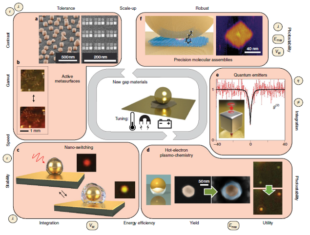
Most interesting is the range of applications in prospect, such as ultimate low-energy devices like robust bottom-up assembled single-atom switches. A summary of these applications can be found in Figure 2.
Author: César Tomé López is a science writer and the editor of Mapping Ignorance
References
- Jeremy J. Baumberg, Javier Aizpurua, Maiken H. Mikkelsen & David R. Smith (2019) Extreme nanophotonics from ultrathin metallic gaps Nature Materials doi: 10.1038/s41563-019-0290-y ↩
1 comment
[…] Espazio txikietan, nanometro kubiko bateko espazioetan, argiarekin gertatzen dena oso interesgarria da. Hainbeste, ezen kontsumo baxuko dispositibo nanometrikoak eta aukera handiak martxan dauden. Javier Aizpurua (CFM &DIPC), nanofotonika aditua, berrikuspena egin du taldekideekin batera. The extreme nanophotonics of the […]