The spin texture of surfaces and electron scattering
The spin texture of surfaces and electron scattering
An electric current can be visualized as a flow of electrons through a conducting piece of material. The less the resistance the material structure opposes to the flow of electrons the better a conductor it is. A part of this resistance appears at the surface of the material, where the electrons first encounter it; as with electromagnetic radiation – electrons are a particle and a wave – electron scattering occurs, and part of the electrons are bounced back to the direction from which they came. This effect, called backscattering, which is a diffuse reflection due to scattering, makes the electric current very sensitive to defects in the material.
The spin-orbit interaction (SOI), between the orbital angular momentum and the spin angular momentum of an electron, can dramatically influence electron scattering on the surface of crystalline compounds to the point of quenching backscattering. The absence of backscattering makes not only an electric current less sensitive to defects in the material, it also facilitates the generation of spin currents, the flow of electron spin. This is most interesting for spintronics applications, where spin currents are the analogues of electric currents in electronics.
When you read about SOI in a textbook, when talking about the fine structure of atomic spectra for example, there is an implicit assumption: there exists a spatial inversion symmetry, i.e., for every point in space (x, y, z) we assume there is another one, completely equivalent, at (-x, -y, -z). When there is in fact inversion symmetry we find SOI common to all types of crystals as it stems from SOI at the atomic orbitals. But what happens if our particular crystal has no inversion symmetry is that, in addition to the standard one, special kinds of SOI appear. And this is the case if we consider surfaces of any crystal. Therefore studying SOI at surfaces is critical to understand electron scattering and the generation of spin currents.
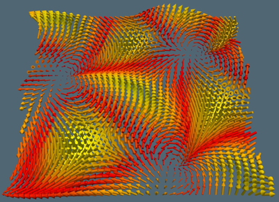
The so called spin texture at the surface is characterized by the Rashba effect, a splitting of the spin-up and spin-down states in energy and momentum, and the effect of SOI at the surface can be qualitatively described by the Rashba-Bychkov model. The Rashba effect, discovered in 1960, was the basis for the spin transistor by Datta and Das in 1990, which has greatly influenced the field of spintronics.
But real materials are much more complex than those depicted in the Rashba-Bychkov model. Now, a group of researchers from the Institut Catalá de Nanociencia i Nanotecnologia and Eugene Krasovskii from UPV/EHU and DIPC, have studied experimentally 1 electron scattering in the surface of BiAg2 alloy, which on the one hand exhibits the largest Rashba effect known to date, and on the other is as far as it can be from the conventional Rashba-Bychkov model. They find a different scattering behaviour associated to the specific localization of the elements that compose the alloy.
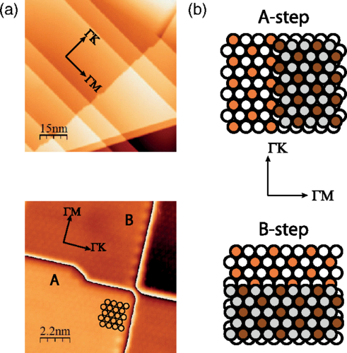
The researchers analysed the scattering patterns produced by atomically straight steps (A and B, see Figure 1) with different concentrations of Ag and Bi atoms. The experiments were performed using a scanning tunnelling microscope (STM) operated at 5 K in ultra-high vacuum on a sample of BiAg2 grown on a silver single crystal.
They found that for A steps, the reflection was strongly asymmetric and that transmission was negligible. These results are similar to those reported for the Ag(111) surface state. The results for B steps, however, are strikingly different. Both reflection and phase shift are symmetric, and there is a substantial transmission.
Schirone et al attribute the different scattering behaviour of each step type to the element-specific localization of wave functions on the BiAg2 bilayer. Moreover they identify a backscattering spin-flip mechanism, not predicted in the usual Rashba-Bychkov framework, highly sensitive to the chemical composition of the step edges due to the different degree of localization of the occupied and unoccupied electronic wave functions on Ag and Bi sites.
The correlation of the scattering properties with the atomic scale chemical composition of the steps implies the existence of a connection between the SOI strength in the scattering region and the probability of backscattering. These results can be generalized to other heterogeneous heavy metal compounds with strong Rashba interaction, and are relevant for engineering possible future spintronics devices based on these materials.
Author: César Tomé López is a science writer and the editor of Mapping Ignorance.
References
- S. Schirone, E. E. Krasovskii, G. Bihlmayer, R. Piquerel, P. Gambardella, and A. Mugarza (2015) Spin-Flip and Element-Sensitive Electron Scattering in the BiAg2 Surface Alloy Phys. Rev. Lett. 114, 166801 DOI: 10.1103/PhysRevLett.114.166801 ↩
1 comment
[…] The analogue of the Hall effect for spin, the spin Hall effect, is the accumulation of particles with opposite spin on the opposite surfaces of a material in which a current is flowing. However, the analogy is not complete […]