The multiscale nature of picocavities: a classical view to a quantum effect
The multiscale nature of picocavities: a classical view to a quantum effect

Progress in nanotechnology has allowed controlling the morphology of metallic nanoparticles at the nanometer and even subnanometer scale, triggering the development of various applications in plasmonics and nanooptics, such as in enhanced vibrational spectroscopy, improvement of energy absorption of solar cells, optoelectronic circuits, quantum optics, nanosensing of biomolecules, or noninvasive thermotherapy in medicine.
Most of the fascinating properties and applications of plasmonic nanoparticles are based on five distinctive characteristics that make surface plasmons (collective electronic oscillations at the surface of metals) attractive: their ability to concentrate light beyond the diffraction limit; their ability to modify the local density of photonic states; their ultrafast response; their environmental sensitivity; and their flexibility in design. In other words, the tunability of their optical response, along with their ability to enhance electromagnetic fields, squeezing the electromagnetic energy down to nanometer scale volumes around sharp tips or at interparticle gaps, produce “hot spots”, behaving as effective optical nanoantennas.
The near-field (close to the antenna) patterns in nanostructures under light excitation strongly depend on the size, composition, and shape of the individual particles, along with plasmon hybridization in coupled nanostructures.
When the size or the separation distance between plasmonic nanoparticles becomes of the order of a few nanometers or even smaller, the quantum nature of the electrons emerges. The effects due to this feature are initially not included in typical local classical electrodynamical descriptions of the optical response, and different levels of approximation have been adopted to address its influence in the response in extended classical models.
In any case, a proper description of the effect of atomic-scale edges, wedges, vertices, and protrusions at surfaces requires a complete quantum theoretical framework, which includes the atomistic structure of the nanoparticles and the wave nature of electrons building up the plasmonic excitations. It is important to note that, at the picoscale, the localization of local fields in atomic-scale cavities boosts the coupling of photons with the electronic transitions of single emitters or with the vibrations of a molecule in optomechanical interactions.
Actually, the quantum description of these optical picocavities at the full atomistic level reveals the importance of atomic-scale features. However, such a detailed description is often limited by the computational requirements, even with the relatively efficient time-dependent density functional theory methods.
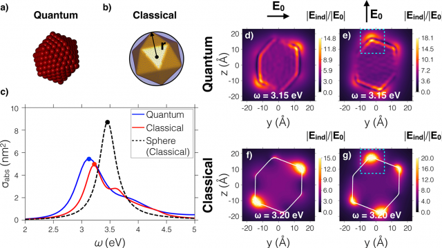
Now, a team of researchers from UPV/EHU, CFM and DIPC propose 1 the use of a simplified local classical approach to address the optical response and the local field distribution around picocavities. The result is a nonresonant lightning rod effect at the atomic scale that produces an extra enhancement over that of the plasmonic background. The new concept impacts nanoscale condensed matter physics, quantum chemistry, and nanophotonics equally.
The researchers perform atomistic, ab initio calculations of the optical response of the nanoparticles based on time-dependent density functional theory. For the classical electromagnetic calculations, they implement the boundary element method within the framework of the local dielectric theory. The investigation focuses on icosahedral sodium clusters for such a comparison, although the method can be extended to other materials and shapes.

Unexpectedly, a lightning rod effect at the atomic scale is identified as responsible for this extra localization, induced by the electrical potential gradient produced by the electronic wave functions of the atomistic features. When superimposed on top of a nanometric plasmonic resonance, the lightning rod effect acts as a multiplier effect, producing an extra factor of field enhancement, which is characterized by a further spatial localization as compared to the supporting resonance, and a similar spectral distribution.
The calculations show that a classical model within the solution of Maxwell’s equations, where the atomic-scale features are described by sharp boundaries following the profile of the electron density associated with the atoms, is able to reproduce very satisfactorily the field localization and the effective mode volume in relevant canonical plasmonic nanoresonators such as in single metallic nanoparticles and in nanometric gaps formed by nanoparticle dimers.
The existence of picocavities in metallic surfaces has probably been unconsciously revealed in many molecular spectroscopy experiments, enhanced by the action of surface plasmons; however, it is now, with the use of a simplified scheme as shown here, that researchers can start to interpret the effects of atomic-scale features in spectroscopic signals in a compact and simple way by properly addressing the multiscale nature of the hosting cavities.
Author: César Tomé López is a science writer and the editor of Mapping Ignorance
References
- Mattin Urbieta, Marc Barbry, Yao Zhang, Peter Koval, Daniel Sánchez-Portal, Nerea Zabala, and Javier Aizpurua (2018) Atomic-Scale Lightning Rod Effect in Plasmonic Picocavities: A Classical View to a Quantum Effect ACS Nano doi: 10.1021/acsnano.7b07401 ↩