Structurally well-defined boundaries in a fully accessible quantum spin Hall insulator
Structurally well-defined boundaries in a fully accessible quantum spin Hall insulator
Imagine that we have a conductor or a semiconductor through which a current is flowing. Then we apply a strong transverse magnetic field. As a result, we can measure a potential difference at right angles to both the current and the field caused by the deflection of charge carriers by the field. This effect was described by Edwin Hall in 1879 and is the classical Hall effect. It introduces a coefficient which is a constant characteristic of the material. A quantum mechanical version of the Hall effect can be found at very low temperatures, in this the Hall coefficient is quantized.
The analogue of the Hall effect for spin, the spin Hall effect, is the accumulation of particles with opposite spin on the opposite surfaces of a material in which a current is flowing. However, the analogy is not complete since an external magnetic field destroys the effect. The spin Hall effect is due to spin-orbit coupling and this coupling can be intrinsic or extrinsic to the material: The intrinsic mechanism is a consequence of the band structure of the material, whereas the extrinsic mechanism stems from scattering of the charge carriers by impurities that locally induce spin-orbit coupling.

Materials exhibiting the quantum spin Hall effect, the so-called quantum spin Hall insulators (QSHI), create new opportunities for directly imaging the spatial extent of topologically protected one-dimensional edge states and for determining how they interact with bulk states and defects. Such systems, however, can be difficult to isolate and to access via microscopy. HgTe and InAs/GaAs quantum wells, for example, are well-known QSHIs but are not easily accessible to high-resolution scanned probe microscopy because they are buried interface systems. On the other hand, Bi-based surface systems (predicted to be QSHIs) have shown evidence for QSHI behaviour and are more accessible to scanned probe microscopy, but exhibit strong substrate interactions.
Monolayer transition metal dichalcogenide materials (MX2 where M= Mo, W, and X = S, Se, and Te) in the distorted octahedral 1T′ phase, on the other hand, are a new class of QSHIs that retain their topological properties on different substrates and are completely accessible to high resolution scanned probe microscopy. Monolayer 1T′-WTe2 films have recently been shown to exhibit all of the hallmarks of the QSH effect (e.g., band inversion, helical edge states, and edge state quantum conduction).
Monolayer 1T′-WTe2, however, poses challenges for quantitative microscopy of topological edge states due to the high degree of structural disorder in the edges of two-dimensional 1T′-WTe2 islands produced by molecular beam epitaxy. Although the existence of topological edge states is protected against disorder, quantitative characterization of their decay lengths, dispersion features, and defect interactions requires crystallographically well-ordered edges since these properties strongly depend on edge orientation, strain, and chemical environment.
Now, Miguel Moreno Ugeda (Ikerbasque Research associate, DIPC, CFM) and collaborators 1 in order to achieve structurally well-defined boundaries in a fully accessible QSHI, have grown mixed-phase WSe2 monolayers on SiC (0001) using molecular beam epitaxy techniques.

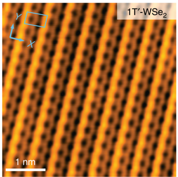
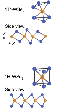
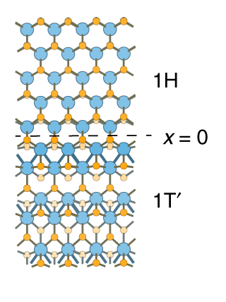
Monolayer WSe2 is bimorphic with two stable crystalline phases, 1H and 1T′ (Figure 1), that are close in energy, thus enabling the growth of mixed topological/trivial phases with crystallographically defined phase boundary interfaces. The 1H phase (which is the structural ground state of WSe2) has a much larger electronic bandgap than the 1T′ phase, thus allowing the two phases to be easily distinguished. The onset of the quantum spin Hall effect in mixed-phase WSe2 results in topologically protected states at crystallographically well-defined 1T′–1H phase boundary interfaces.
The researchers then could verify the QSHI ground state of 1T′-WSe2 using ARPES, STM/STS, and first-principles calculations. ARPES reveals the existence of inverted bands at the Fermi energy (EF) and the presence of a bulk bandgap. STS measurements confirm the bulk bandgap seen by ARPES and further demonstrate the existence of topological interface states within this bandgap that are spatially localized at 1T′-WSe2 boundaries. These boundary states are easily observable at crystallographically well-ordered 1T′–1H interfaces, but can also be seen at the irregular 1T′ edges.

The structural perfection of the 1T′–1H boundary allowed to measure an interface state decay length of 2 nm into bulk 1T′-WSe2, agreeing with the results of ab initio numerical simulations. In other words, measurements support the results of first principles calculations and provide evidence for the presence of the QSHI phase in single-layer 1T′-WSe2.
Hence, the ability to observe one-dimensional interface-states at atomically well-ordered boundaries between trivial and nontrivial phases allows to extract new quantitative information on these novel states, such as their penetration depth into the 1T′-WSe2 bulk, a previously inaccessible parameter due to edge disorder. This creates new opportunities for investigating topologically non-trivial electronic phases in two-dimensional transition metal dichalcogenide materials.
Author: César Tomé López is a science writer and the editor of Mapping Ignorance.
References
- Miguel M. Ugeda et al (2018) Observation of topologically protected states at crystalline phase boundaries in single-layer WSe2. Nature Communications doi: 10.1038/s41467-018-05672-w ↩
1 comment
[…] Los materiales en los que aparece el efecto Hall cuántico de espín son interesantes. Tras este trabajo de la gente del DIPC resultan ser mucho más interesantes: Structurally well-defined boundaries in a fully accessible quantum spin Hall insulator […]