Introducing impurities
Introducing impurities
The most extensive use of semiconductors, such as silicon or germanium, including their use as transistors, arises from their behavior when, after being sufficiently purified of atoms other than the basic element (e.g., silicon or germanium), very small amounts of special impurities are carefully introduced.
While the methods for first purifying then adding small amounts of impurities to germanium became available after World War II, research on the purification and controlled introduction of impurities for silicon did not succeed until the late 1950s. Since silicon is more abundant than germanium and other semiconductors, it soon replaced germanium as the preferred semiconductor.
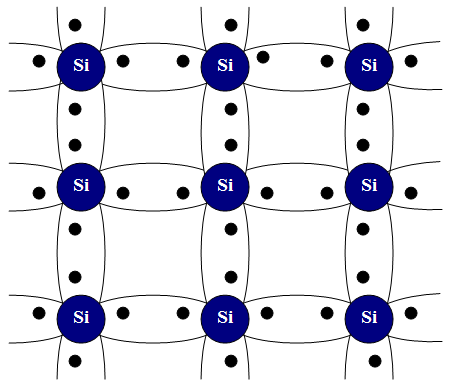
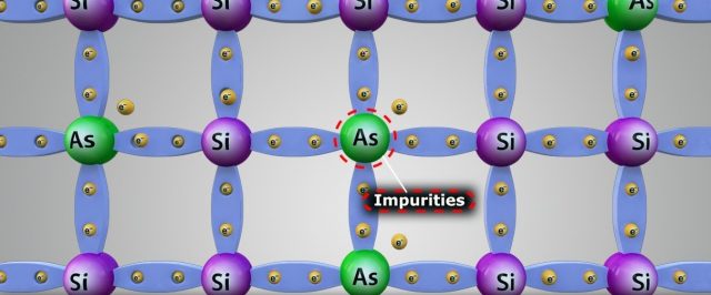
Germanium (element 32) and silicon (element 14) each have four valence electrons, which fill up the valence band when these metals form a crystal. Element 33, arsenic, has five valence electrons, as does element 15, phosphorus. If a very small amount of arsenic is added to germanium as the germanium crystal is formed, the arsenic atoms will substitute for a germanium atom in the lattice. The same happens when a small amount of phosphorus is added to silicon. The small amounts are carefully controlled in the production process and are only about 0.0001% of the total atoms. This process is called doping, and the impurities are called dopants.
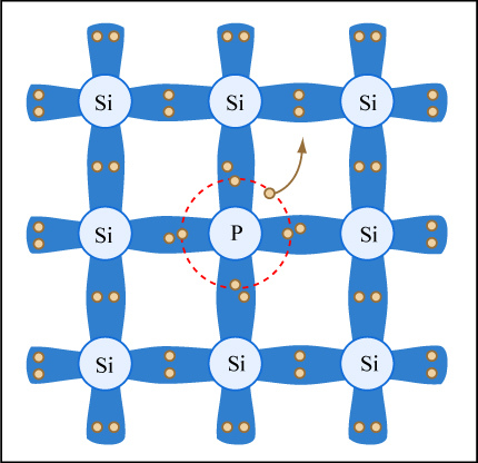
When the corresponding dopant is introduced into the germanium or silicon lattice, four of its valence electrons are bonded to the other atoms in the lattice, leaving the fifth valence electron without a bond. These extra valence electrons from the dopants are so lightly attached to their atoms that they easily absorb vibration energy (phonons) and jump into the conduction band of the semiconductor. At room temperature they are all in the conduction band, which means that the doped semiconductor now acts like a full conductor.
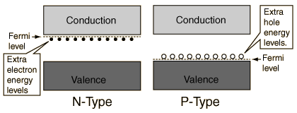
Since the negative electrons donated by the impurities enable the material to conduct, these types of semiconductors are called n-type semiconductors. A similar situation occurs when the semiconductors are doped with impurities one space lower on the periodic table, that is when silicon (14) is doped with element 13, aluminum, and germanium (32) is doped with element 31, gallium. The dopants have only three valence electrons. So, when they are bound into the silicon or germanium lattice, they leave a space in the valence band indicating that they are able to accept an electron from a neighbouring silicon or germanium atom. This space is called a hole.
The hole behaves similarly to an air bubble in a glass of soft drink or beer. When an external electric field is turned on, electrons from the neighbouring atoms, which normally cannot move anywhere, can now move over one atom in filling up the hole. But then this leaves a hole in the neighbouring atom, which can be filled up by its neighbour, and so on. Similarly, the upward motion of the air bubble in a glass of beer actually involves the downward flow of beer into the space occupied by the bubble, which appears to the eye to be moving upward. In the semiconductor, if the field moves the electrons to the left in the diagram, the hole appears to migrate to the right. By moving to the right, it is behaving like a positive charge, even though it is just a space.
Nevertheless, because of the motion of negative charge to the left, the physical effect is the same as if positive charges were flowing to the right in the valence band, below the conduction band, where previously no charges could flow at all. Once again, the very careful introduction of small amounts of impurities has turned the semiconductor into a full conductor. Since the conducting charges appear to be positive, this is known as a p–type semiconductor.
These doped semiconductors could be used like any other conductor, but that is hardly worthwhile, since we can produce full conductors much more easily and cheaply, for example, copper wires. Instead, it was recognized during and after WWII that the really useful applications of these types of semiconductors is when they are placed physically next to each other inside electronic devices.
References:
Asimov, I. (1993) New Guide To Science Penguin Press Science
Cassidy, D. et al (2002) Understanding Physics Springer Verlag New York
Kuphaldt, T.R. (2009) Lessons in Electric Circuits, Volume III: Semiconductors
Nave, C.R. (2012) HyperPhysics
Author: César Tomé López is a science writer and the editor of Mapping Ignorance.