How to build structures atom by atom using a scanning transmission electron microscope
How to build structures atom by atom using a scanning transmission electron microscope
“What would happen if we could arrange the atoms one by one the way we want them?”
Richard Feynman

Fabrication of matter atom by atom remains a long-standing dream and ultimate goal of nanotechnology, following the famous challenge by Feynman 58 years ago. For 30 years, the atom-by-atom fabrication remained the province of visionary thinking and science fiction, inspiring but seemingly unachievable given the then available fabrication tools. The situation changed drastically upon the introduction of scanning tunneling microscopy (STM) by Binnig and Rohrer and subsequently STM-based atomic fabrication by Eigler.
This advancement immediately riveted the attention of both the scientific and general community worldwide, launching the era of nanotechnology. It also started the developments of technologies based on combined STM and surface science methods, ultimately leading to the development of single-atom qubit devices.
Despite the remarkable progress in STM-based atomic fabrication, the fabrication process remains slow and requires complex surface science approaches to establish and maintain atomically clean surfaces. This process further requires a complex technological cycle to integrate single-atom devices with the classical semiconductor technologies. Correspondingly, the development process remained slow and required large capital investments to even begin the development. Thus, alternative methods for atom-by-atom fabrication are most interesting.
Enter the electron microscope, a form of microscope that uses a beam of electrons instead of a beam of light (as in an optical one) to create a large image of a very small object. In recent years, the ever-growing body of work in high-resolution scanning transmission electron microscopy has illustrated the potential of the electron beam (e-beam) to induce local atomic-scale changes in materials microstructure that can be immediately visualized. The e-beam, then, could be used for the fabrication of atomic-scale structures.
Following these predictions, developments followed step by step. First, a controllable e-beam induced the movement of a single silicon atom (Si) a short distance through a graphene lattice. This was accomplished through spot irradiation of a carbon atom (C) adjacent to a dopant Si. Occasionally the C atom receives a large enough impact (≈15 eV) from the beam to induce a bond reversal where the Si and C switch places in the lattice. It follows that, repeating this technique, an atom may be controllably moved step by step through the graphene lattice. Then, the energy required for various processes involved in atomic motion and the creation of point defects was calculated. Additional studies served to clarify various atomic-scale processes and transformations in graphene. Finally, an approach was found to incorporate single Si dopants into the graphene lattice at preselected locations, localizing single-dopant atoms at specific lattice sites.
Based on these studies, an international team of researchers, including Elisa Jimenez-Izal and Anastassia N. Alexandrova, both from UPV/EHU and DIPC, felt ready to further develop atomic-scale control and, critically, demonstrate atom-by-atom assembly by electron beam manipulation.
They have published the results of their work, where controlled manipulation and assembly of a few atom structures are demonstrated 1 by bringing together single atoms using a scanning transmission electron microscope.

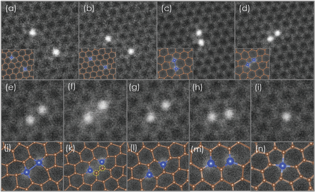
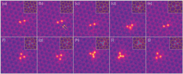
The team uses an atomically focused electron beam to introduce Si substitutional defects and defect clusters in graphene with spatial control of a few nanometers and enable controlled motion of Si atoms (Figure 1). The Si substitutional defects are then further manipulated to form dimers, trimers, and more complex structures. All this beam-induced atomic-scale chemical process dynamics is captured in a time-series of images at atomic resolution (Figure 2).
The researchers demonstrate that directing a 100 keV focused electron beam across the source material and the graphene lattice can reliably generate multiple substitutional Si defects. Subsequent manipulation of the introduced defects may be accomplished by decreasing the microscope accelerating voltage to 60 kV and using controlled scan areas or direct stationary beam irradiation to induce movement (Figure 3). DFT modeling was performed to more clearly understand the structures formed, the energies required to form them, and explore other possible stable structures.

Other dopants are possible, though. While this work examines specifically Si dopants in graphene, a variety of other dopants have been observed in/on graphene, including B, N, O, P, Fe, Au, Cr, Ti, Pd, Ni, and Al, with P also showing e-beam-induced movement through the lattice (though only a very short distance).
On the other hand, also a variety of two-dimensional materials in addition to graphene may provide opportunities for e-beam mediated atomic alterations, for example, transition metal dichacogenides (TMDs). Such precise tailoring may enable in situ fabrication of some sophisticated materials, such as graphene quantum dots embedded in hexagonal boron nitride (h-BN) or graphane-based spin current diodes.
These studies suggest that control of the e-beam-induced local processes offers the next step toward atom-by-atom nanofabrication, providing an enabling tool for the study of atomic-scale chemistry in 2D materials and fabrication of predefined structures and defects with atomic specificity.
Author: César Tomé López is a science writer and the editor of Mapping Ignorance.
References
- Ondrej Dyck, Songkil Kim, Elisa Jimenez-Izal, Anastassia N. Alexandrova, Sergei V. Kalinin, and Stephen Jesse (2018) Building Structures Atom by Atom via Electron Beam Manipulation Small doi: 10.1002/smll.201801771 ↩