An experimental protocol for two-probe scanning tunneling microscopy
An experimental protocol for two-probe scanning tunneling microscopy
A region containing a maximum of potential that prevents a particle on one side of it from passing to the other side is called a potential barrier. The net in a tennis court is in a certain way a potential barrier, as the ball needs to have kinetic energy in excess of the height of the potential barrier to pass it. This is a macroscopic example that obeys classical physics.
A potential barrier sorrounds the atomic nucleus and is important in nuclear physics; a similar but much lower barrier exists at the interface between semiconductors and metals and between differently doped semiconductors. As you can imagine, these barriers are important in the design of electronic devices. However, at this level quantum effects are extremely important. And it is the case that in the quantum world there is a non-zero and finite probability that a particle with less energy will pass through the barrier. This is the tunnel effect.
Scanning tunneling microscopy (STM) is a technique in which a fine conducting probe is held close to the surface of a sample. Electrons tunnel between the sample and the probe, producing an electrical signal. The probe is slowly moved across the surface and raised and lowered so as to keep the signal constant. The precision reached in approaching the STM tip apex toward the surface permits for a controlled electronic contact with a single surface atom or molecule. A profile of the surface is thus produced, and a computer-generated contour map is created.
The invention of the scanning tunneling microscope by Binnig et al. in 1982 opened a new era in surface science. It is now a standard microscopy technique for real-space imaging of the electronic structure of conducting surfaces with picometer resolution. Single-probe STM is also a spectroscopic tool, able to locally probe electronic surface states as a function of the bias voltage in the scanning tunneling spectroscopy (STS) mode. Thus, vertical contacts formed by STM can be used to study electronic transport through adsorbates with atomic-scale lateral resolution.
However, the direct determination of the electronic transport properties of a planar atomic-scale wire or circuit lies beyond the single-probe approach. This requires fabricating metal contacts with such a high precision that it becomes a real challenge. An attractive alternative is the use of multi-probe STM. This method offers a high control on the position and geometry of the contacts between the probes and the nanoscale system. But the downscaling of multi-probe instruments toward the atomic level, i.e., where all STM tip apex positions are controlled at the atomic scale, meets many technical obstacles of its own. Actually, only recently two-probe STM experiments have reached the required atomic precision in contacting structures on a surface. Even though that technical result made atomic-scale two-probe STM experiments feasible, to date no experimental protocols for extracting transport properties of atomic structures from such experiments have been reported.

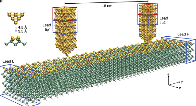
Now, an international team of researchers, including members from CFM and DIPC, has investigated 1 electronic transport along the anisotropic germanium (001) surface with the use of two-probe scanning tunneling spectroscopy and first-principles transport calculations. They directly observe quasi-one-dimensional electronic transport channels provided by the unoccupied surface states running along the dimer rows on the Ge(001) surface. Understanding the transport properties of this surface is important, as it provides an excellent platform for fast and reliable fabrication of atomic-scale circuits.
The Ge(001) surface consists of buckled Ge dimers forming well-separated parallel rows. The existence of surface dangling bonds introduces additional unoccupied states within the band-gap of the bulk Ge electronic structure. Importantly, weak interactions between adjacent rows result in strong anisotropy of this band structure. Consequently, the reconstructed dimer rows on the bare Ge(001) surface form a series of parallel quasi-1D wires.
The researchers introduce a method for the determination of the transconductance in the two-probe experimental setup and demonstrate that it captures energy-resolved information about electronic transport through the unoccupied surface states.
The sequential opening of two transport channels within the quasi-one-dimensional Ge dimer rows in the surface gives rise to two distinct resonances in the transconductance spectroscopic signal, consistent with phase-coherence lengths of up to 50 nm and anisotropic electron propagation.
The new protocol can be used to characterize transport at the nanoscale in planar atomic-scale devices and two-dimensional materials grown on surfaces. In contrast to standard metal contacts, e.g., fabricated by lithographic techniques, the use of two-probe STM enables a precise adjustment of individual atomic contacts and their resistances. This additional level of control helps to access the system’s intrinsic transport properties, disentangling them from those of the contacts and leads.
Author: César Tomé López is a science writer and the editor of Mapping Ignorance.
References
- Marek Kolmer, Pedro Brandimarte, Jakub Lis, Rafal Zuzak, Szymon Godlewski, Hiroyo Kawai, Aran Garcia-Lekue, Nicolas Lorente, Thomas Frederiksen, Christian Joachim, Daniel Sanchez-Portal & Marek Szymonski (2019) Electronic transport in planar atomic-scale structures measured by two-probe scanning tunneling spectroscopy Nature Communications doi: 10.1038/s41467-019-09315-6 ↩