Proximity effects or the fragility of electronic ground states in 2D materials
Proximity effects or the fragility of electronic ground states in 2D materials
Transition metal dichalcogenides (TMDs) are layered compounds which can be thinned down to the single-layer limit. While mechanical exfoliation generates atomically thin TMD flakes possessing an area of a few square microns, chemical and physical methods provide high-quality monolayers on large-area substrates, which are suitable for actual technological applications.
TMDs are a class of van der Waals layered materials, an ideal playground for the investigation of exotic electronic phases in two dimensions due to greatly enhanced many-body interactions. Thus, TMDs exhibit a rich variety of electronic phases such as charge density wave (CDW) order, superconductivity, quantum spin liquid, magnetism, and, even, topological phases. In metallic TMDs (MX2 with M = Nb, Ta, Ti, V, Sn and X = S, Se, Te), CDW order and superconductivity are frequently present from the bulk form down to the single-layer limit, although with rather disparate properties in many cases.
Importantly, most of these electronic states rely on the strength of electron−electron and electron−phonon correlations and, therefore, are significantly sensitive to variations in the electronic and phonon band structures. Such fragility becomes critical in the single-layer limit since the entire crystal lattice is exposed to the environment and many external factors can therefore affect their stability. Perhaps the most influential factor on the properties of 2D materials is the presence of the substrate, as it often triggers numerous “proximity effects”. So far, CDW
and superconducting orders have been studied in epitaxial TMD layers on substrates that do not necessarily minimize their potential impact on the properties of the TMD layer but instead are suitable for a high quality growth of the TMD. These are mainly noble metals such as gold and doped graphene surfaces. But what happens with other substrates?
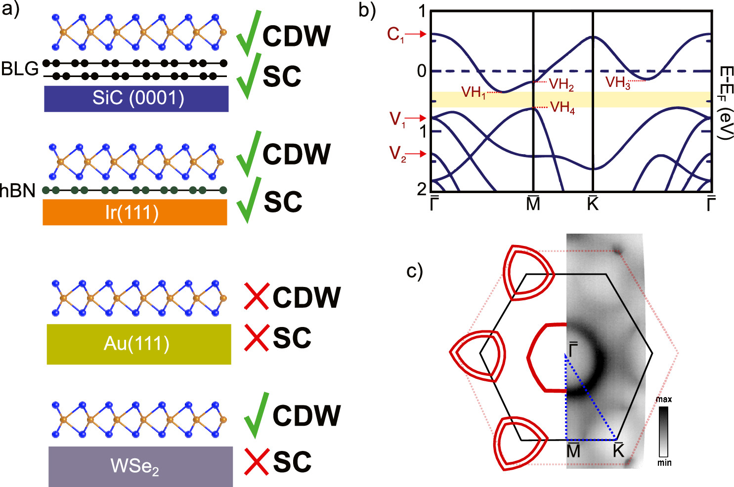
Now, a team of researchers assesses 1 the impact of different substrates on the CDW and superconducting phases as well as the electronic structure of a model correlated 2D material. In particular, the team studies the electronic ground state of high-quality single-layer NbSe2 grown by molecular beam epitaxy on four substrates with markedly distinct structural and electronic nature: bilayer graphene/SiC(0001), single-layer boron nitride (h-BN)/Ir(111), Au(111), and bulk WSe2. By combining low-temperature (340 mK) scanning tunneling microscopy/spectroscopy and angle-resolved photoemission spectroscopy, we compare the electronic structure of this prototypical 2D
superconductor on each substrate.
The results are astounding. Even though the electronic structure of single-layer NbSe2 remains largely unaffected in all cases – except for a nonuniform shift of the band structure on Au(111) – while both CDW and SC persist with nearly identical properties on bilayer graphene/SiC(0001) and h-BN/Ir(111), they are absent or, at least, severely weakened on Au(111) and bulk WSe2 .
These results show, in quite a dramatic way, the power of proximity effects of the substrates or, if you prefer, the fragility of electronic ground states in 2D materials.
Author: César Tomé López is a science writer and the editor of Mapping Ignorance
Disclaimer: Parts of this article may have been copied verbatim or almost verbatim from the referenced research paper/s.
References
- Paul Dreher, Wen Wan, Alla Chikina, Marco Bianchi, aojie Guo, Rishav Harsh, Samuel Mañas-Valero, Eugenio Coronado, Antonio J. Martínez-Galera, Philip Hofmann, Jill A. Miwa, and Miguel M. Ugeda /2021) Proximity Effects on the Charge Density Wave Order and Superconductivity in Single-Layer NbSe2 ACS Nano doi: 10.1021/acsnano.1c06012 ↩