Engineering quantum states and electronic landscapes
Engineering quantum states and electronic landscapes
Surfaces are at the frontier of every solid. They provide versatile supports for functional nanostructures and mediate essential physicochemical processes. Intimately related to two-dimensional materials, interfaces and atomically thin films often feature distinct electronic states with respect to the bulk, which is key to many relevant properties, such as catalytic activity, interfacial charge-transfer, and crystal growth mechanisms. Both atomic manipulation and supramolecular principles provide access to custom-designed molecular assemblies and superlattices, which tailor the surface electronic landscapes and influence fundamental chemical and physical properties at the nanoscale.
Once the foundations of atomic and molecular sciences were established, reaching an atomistic understanding of matter and trying to control it at the atom level was the natural next step. In this vein, enormous effort has been dedicated to developing fabrication, characterization, and manipulation procedures, providing access to novel expressions of materials, useful electronic, photonic, or magnetic properties, as well as collective atomic states with ever-increasing precision and complexity.
Multiple instrumental developments were crucial to providing direct insight into the nature and behaviour of atomic and molecular species at the angstrom scale, whereby the imaging capabilities by electron microscopy, field-ion microscopy (FIM), scanning tunnelling microscopy (STM), and noncontact atomic force microscopy (NCAFM) techniques proved to be of significant value. Prominent direct visualization of crystal surface atomic lattices and adsorbed species were first achieved by FIM and subsequently with the more versatile STM, generating revolutionary scientific insights.
Using cryogenic STM, addressing and positioning individual atoms became a reality and was immediately recognized as an iconic achievement in nanoscale science. Likewise, insights into the essential electronic structure of materials were provided by means of local scanning tunnelling spectroscopy (STS) and space-averaging high-resolution spectroscopies, notably including angle-resolved photoemission (ARPES). The combination of these powerful tools, ideally complemented with theoretical modelling, is an asset to fully characterize electronic properties and their implications
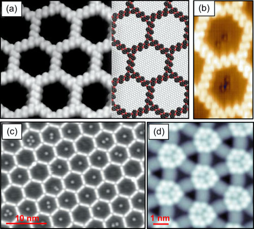
Bottom-up construction procedures were developed to design a wide variety of nanosystems amenable to scanning probe and space-averaging scrutiny. In particular, since the turn of this century, supramolecular chemistry principles have been increasingly employed to create low-dimensional functional nanostructures at well-defined interfaces.
The extensive activities devoted to the exploration of quantum confinement and quasiparticle scattering at nanostructures on metal surfaces promoted the advancement of condensed matter research. This progress is now reviewed 1 by a team of researchers. With the surface states of coinage metals taken as an exemplary playground, the researchers revisit how the design of appropriate nanoarchitectures customizes the electronic structure and topology of the outermost layers.
The team discusses the generally relevant aspects underpinning the scattering and confinement phenomena of two-dimensional electron gases existing at appropriate surfaces, listing prominent cases where firm control over such gases is exerted.
Electronic structure changes by artificial lattices affording exotic properties are also covered. Dirac cones or flat bands, topological edge states, fractal behaviour, and Penrose tiling quasicrystals, some of which mirror the interesting physics of Bose-Einstein condensates, are some of them.
The team concludes that the designed scattering potential landscapes can be described with semiempirical models, bringing thus the prospect of total control over surface electron confinement and novel quantum states within reach.
More on the subject:
Electronic engineering of quantum dot arrays
Engineering hybrid graphene nanoribbons with active electronic properties
Author: César Tomé López is a science writer and the editor of Mapping Ignorance
Disclaimer: Parts of this article may have been copied verbatim or almost verbatim from the referenced research papers
References
- Ignacio Piquero-Zulaica, Jorge Lobo-Checa, Zakaria M. Abd El-Fattah, J. Enrique Ortega, Florian Klappenberger, Willi Auwärter, and Johannes V. Barth (2022) Engineering quantum states and electronic landscapes through surface molecular nanoarchitectures Rev. Mod. Phys. Doi: 10.1103/RevModPhys.94.045008 ↩