Building chips up: wafer-scale, MoS₂ electronics for BEOL integration
Building chips up: wafer-scale, MoS₂ electronics for BEOL integration
Authors: Carlos Márquez & Jorge Ávila are researchers at Nanoelectronics Graphene and 2D Materials Laboratory, CITIC-UGR, Department of Electronics, University of Granada
When we think of faster, cheaper electronics, we usually think “smaller transistors.” But the future is also about stacking—adding new layers of components on top of finished silicon chips. That’s called back‑end‑of‑line (BEOL) integration, and it only works if everything you add can be made at low temperatures (generally below ~400–450 °C), otherwise you damage the wiring, semiconductors and dielectrics already on the chip.
Why BEOL compatibility matters
Modern chips already pack billions of transistors in two dimensions. To keep performance climbing, one promising route is monolithic 3D integration: add memory, sensors, or accelerators above the finished logic, then connect everything vertically. The catch is the temperature ceiling; go much above ~400 °C and you risk diffusing copper and degrading low‑k dielectrics. That’s why BEOL‑friendly materials and processes are critical for next‑generation integration schemes.
MoS₂ as a candidate material
Molybdenum disulfide (MoS₂), a 2D semiconductor only a few atoms thick, offers an intriguing balance of properties. Unlike graphene, it has a band gap, which means it can switch current on and off—exactly what transistors need. And because it belongs to the family of layered transition metal dichalcogenides, it can be synthesized and processed at lower temperatures than conventional semiconductors, making it well suited for BEOL integration. But making uniform films and devices across full wafers—and doing so in a way that plays nicely with existing CMOS—has been the sticking point.
Wafer-scale
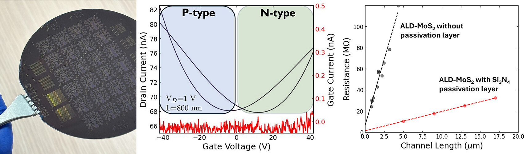
In our latest work, we demonstrate a wafer‑scale, BEOL‑compatible route to make ambipolar MoS₂ transistors—devices that can conduct with either electrons (n‑type) or holes (p‑type)—by using plasma‑enhanced atomic layer deposition (PEALD) 1. Crucially, this is done directly on the target wafer (no delicate crystal transfer), with a thermal budget that respects BEOL limits.
Ambipolar transport matters because it enables complementary logic, where both n‑ and p‑type transistors can be built from the same 2D material. That capability opens the door to efficient logic circuits in stacked, 3D architectures. Achieving this at full wafer scale, with standard microfabrication tools, shifts the field from one‑off demonstrations toward pathways to manufacturing.
One molecular layer at a time
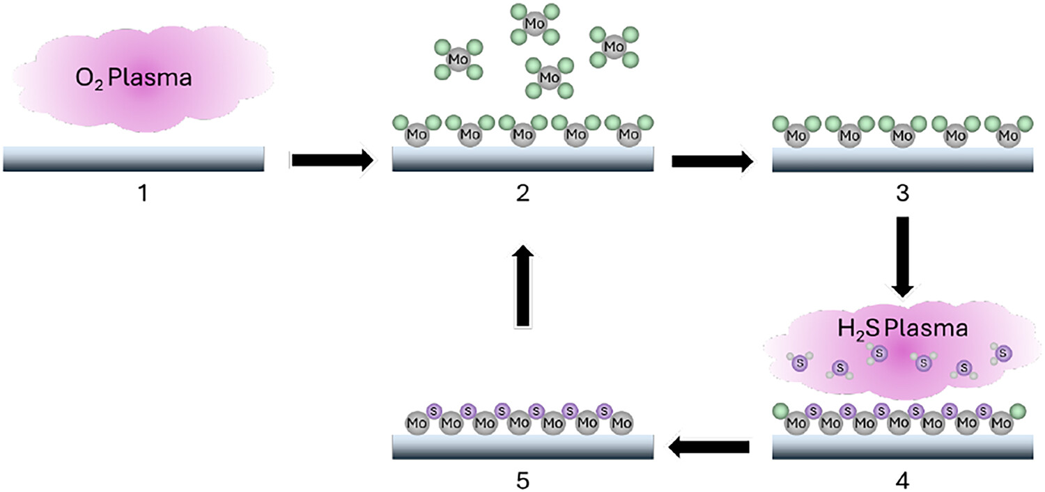
Atomic layer deposition (ALD) grows materials one molecular layer at a time, giving exquisite control over thickness and uniformity across large areas. Using plasma‑enhanced ALD helps at low temperatures by providing extra energy from the plasma rather than from heat. This approach enables device‑grade MoS₂ directly on wafers within the BEOL thermal budget.
The result is back‑gated MoS₂ field‑effect transistors showing ambipolar transport—evidence that both types of charge carriers can be efficiently injected and modulated—fabricated with standard, scalable steps compatible with CMOS back‑end processing. No flake‑by‑flake assembly. No high‑temperature anneals that would cook the interconnect stack.
Integrating emerging materials
This work fits a growing push to co‑integrate emerging materials with mainstream silicon. Low‑temperature 2D devices that can be patterned lithographically and grown across entire wafers open doors to: on‑chip sensors, memory elements, or AI accelerators stacked over compute cores; and to hybrid systems where each layer uses the best material for the job.
References
- A. Martínez, C. Márquez, F. Lorenzo, F. Gutiérrez, M. Caño‑García, J. Ávila, J. C. Galdón Gil, R. Ortega Lopez, C. Navarro, L. Donetti, F. Gámiz. (2025) Wafer‑Scale Demonstration of BEOL‑Compatible Ambipolar MoS₂ Devices Enabled by Plasma‑Enhanced Atomic Layer Deposition. ACS Applied Materials & Interfaces. doi: 10.1021/acsami.5c12014. ↩