Quantifying the screening of electrons in graphene heterostructures
Quantifying the screening of electrons in graphene heterostructures

Beginning in 1928, Felix Bloch, an assistant to Werner Heisenberg in Leipzig, began to make some realistic assumptions in an attempt to formulate a more complete quantum mechanics of electrical conductivity. First, because he wanted to assign a definite momentum and energy to each of the electrons, but not a definite position or a time interval, he chose the wave side of the wave-particle duality. He assumed that the electrons behave, not like particles, but like infinitely extended de Broglie waves. As a result, Bloch did not treat electrons inside metals as a “gas” of particles, but rather as periodic waves extending throughout the periodic crystal lattice. This, it later turned out, helped to explain how electricity can begin to flow in a wire the instant a wire is plugged into a wall socket. If the electrons are viewed as balls of matter, it would take a small amount of time for the current to begin flowing at the rate specified by Ohm’s law.
Bloch made a second assumption. He assumed that the positive metal ions, which are arranged in an infinite, periodic array (that is, in a perfect crystal), each exerts an attractive electric force on the negative electrons. This attractive force formed in visual terms a potential energy that looked like a type of “potential well.” The wells of neighbouring ions then overlapped so that together they formed a periodic arrangement that gave the electron waves a very bumpy ride down the wire.

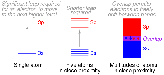
Bloch then solved the Schrödinger equation for the energies that these types of de Broglie waves (wave functions) could possess while moving in this type of periodic potential. He discovered that the allowed energies of the electrons in the material are joined together into bands of quantum states, just as there are certain quantum stationary states within each atom in which the electrons are allowed to exist. Between the bands, as between the quantum states, there is a range of energies in which electrons are forbidden to exist. The bands in the material are actually created by the joining together of the quantum states of the individual atoms. In fact, if there are a total of N identical atoms in the material, then there are N quantum states within each band. According to a rule in quantum mechanics (the Pauli exclusion principle), only two electrons are allowed to occupy any one quantum energy state of a single atom, and this is allowed only because the two electrons spin on their axes in opposite directions.
The electronic band structure is the key to most properties of crystalline materials. Band structure measurements are, therefore, widely used to study the subtle interplay of electrons with lattice excitations or collective electron phenomena. As the bands and their dispersions originate from the quantum overlap between the electronic states of the atoms that make up the crystal, as we have just seen, the coupling between the electron systems of the individual layers of materials where van der Waals interactions are possible is encoded in their band structure. These van der Waals interactions include electrostatic attractions between molecules with permanent dipoles, attractions between dipoles and induced dipoles, and dispersion forces arising because of small instantaneous dipoles in atoms.
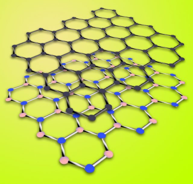
This is important because some heterostructures of graphene and hexagonal boron nitride, a system where van der Waals interactions are possible, are widely used to screen electrons in graphene from the environment, thus providing high electron mobility. In doing so, it is assumed that the two materials are isolated over the full energy range, although small changes in the graphene band structure are observed as a function of the stacking angle of graphene and hexagonal boron nitride. But, is this assumption realistic?
In order to answer that question, Eugene E. Krasovskii, an Ikerbasque professor working at UPV/EHU and DIPC, within a team of researchers have scrutinized 1 the band structure of graphene– hexagonal boron nitride heterostructures over a wide energy range. And they found that the answer is yes.
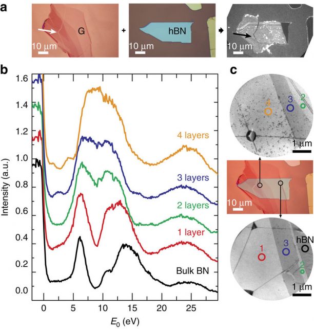
The scientists apply a series of experimental techniques based on low-energy electron microscopy (LEEM) to assess structural and electronic properties in situ, with high lateral resolution. First, they study the band structures of graphite and bulk hexagonal boron nitride as a reference. Combining LEEM-based angle-resolved photoemission spectroscopy (ARPES) and angle-resolved reflected-electron spectroscopy (ARRES), they deduce information on both the occupied and unoccupied bands over an unprecedented energy range. Then the check the band evolution in few-layer hexagonal boron nitride and show that their ARRES data match very well with ab initio calculations.

Once all the previous data are gathered, they focus on stacks of few-layer graphene on hexagonal boron nitride to study their electronic coupling. And they find that despite their similar symmetry and energy range the interlayer states of graphene and do not interact electronically.
The methods used for this work, specifically ARRES, are directly applicable to more complex van der Waals materials, like stacks including transition-metal dichalcogenides, facilitating the study of the (lack of) electronic overlap between the layers quantitatively. In other words, it will be possible to quantitatively understand the ‘chemistry of layers’ by which novel materials are created via electronic coupling between the layers they are composed of.
Author: César Tomé López is a science writer and the editor of Mapping Ignorance
References
- Johannes Jobst, Alexander J.H. van der Torren, Eugene E. Krasovskii, Jesse Balgley, Cory R. Dean, Rudolf M. Tromp & Sense Jan van der Molen (2016) Quantifying electronic band interactions in van der Waals materials using angle-resolved reflected-electron spectroscopy Nat. Comm. doi: 10.1038/ncomms13621 ↩