A Talbot carpet of electrons in nanoporous graphene
A Talbot carpet of electrons in nanoporous graphene

Controlling electron waves by harnessing phase-coherence and interference effects is a cornerstone for future nanoelectronics or quantum computing. To this end, design of platforms with well-defined, narrow, and low-loss propagation channels is essential. Nanoporous graphene (NPG) holds great potential for distributing and controlling currents on the nanoscale. But the effects derived from the wave nature of electrons represent a challenge.
But first things first. What exactly is NPG and why is it interesting?
Graphene is a two-dimensional allotrope of carbon made of hexagons. It is a zero-gap semimetal with a tiny overlap between valence and conductance bands. Since the isolation of graphene in 2004, considerable interest has been paid to exploring its applications in a variety of fields such as electronics, composites, sensors, catalysis and energy related systems. But, in order to facilitate the implementation of a graphene-based device, an essential change of the electronic structure of graphene must be achieved first – namely, the controlled creation of a band gap.
Two fundamentally different mechanisms are known to be able to do just that: a sublattice symmetry breaking or an induced strong spin−orbit interaction. The band gap appearance can drive graphene into a narrow-gap semiconductor if we use the first.
Processing graphene into nanoribbons – strips of graphene – with widths of less than 10 nm can open up a band gap that is sufficient for room temperature field effect transistor applications. Unfortunately, graphene nanoribbon-based devices often have low driving currents, making them unsuitable for practical applications.
Enter nanoporous graphene (NPG), a unique graphene nanostructure that can be regarded as a densely interconnected network of multiple nanoribbons Through the formation of NPGs it is possible to open an energy band gap in a large area graphene sheet to generate a semiconducting thin carbon film. By achieving bottom-up synthesis and transfer of atomically precise NPGs, Moreno et al. (2018) have recently paved the way for the fabrication of high-quality NPG-based devices.
Now, what is the challenge?
We know that particles have two aspects, particle and wave. We usually think of electrons as particles but they can also be regarded as waves, as they do behave like waves. And waves, interact with objects and with themselves giving way to well-known phenomena, like diffraction or interference. The particulars of the phenomena depend on the medium the wave is travelling through.
The point is that electrons in graphene – the medium in this case – can show diffraction and interference phenomena fully analogous to those of light. It is not clear, though, how this optical analogy persists in a nanostructured graphene like NPG. This is so because the particular edge topology of the linked graphene nanoribbons making up the NPG results in a pronounced in-plane anisotropy, which is reflected in the electronic structure.
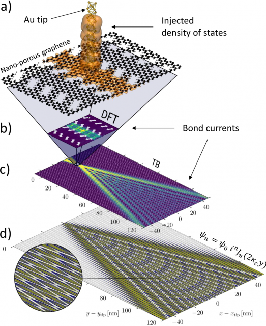
Now, an international team of researchers, including Ikerbasque Research Professor Thomas Frederiksen (DIPC) and Ikerbasque Research Associate Arantzazu Garcia Leuke (DIPC), has theoretically investigated 1 to what extent currents can be injected along individual graphene nanoribbons channels in gated NPG-based devices that have a chemical contact with a scanning tunneling microscope probe.

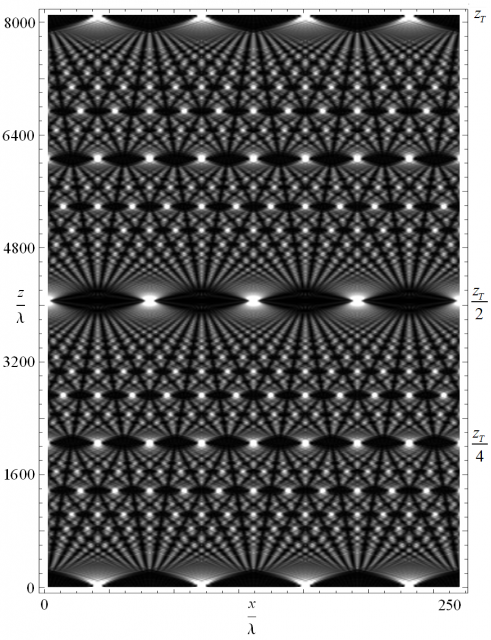
The researchers develop a multiscale method based on density functional theory and non-equilibrium Green’s functions, enabling current calculations with devices longer than 100 nm, relevant for experiments. They find that the inter-nanoribbon coupling disrupts the longitudinal electron confinement into individual channels, giving rise to the Talbot effect (Figure 1), a fascinating interference phenomenon predicted to occur in discrete optical waveguide systems.
The Talbot effect is a near-field diffraction effect first observed in 1836 by Henry Fox Talbot. When a plane wave is incident upon a periodic diffraction grating, the image of the grating is repeated at regular distances away from the grating plane. Lord Rayleigh showed that the Talbot effect was a natural consequence of Fresnel diffraction.
The authors link the origins of this interference phenomenon to the band structure of the NPG. They also demonstrate how the Talbot effect may be detected experimentally using dual-probe scanning tunneling microscopy. This is most important as Talbot interference of electron waves in NPG or other related materials may open up new opportunities for future quantum electronics, computing, or sensing.
Author: César Tomé López is a science writer and the editor of Mapping Ignorance.
References
- Gaetano Calogero, Nick R. Papior, Bernhard Kretz, Aran Garcia-Lekue, Thomas Frederiksen, and Mads Brandbyge (2019) Electron Transport in Nanoporous Graphene: Probing the Talbot Effect Nano Letters doi: 10.1021/acs.nanolett.8b04616 ↩