A universal base geometry for probing 2D semiconductor layers
In nanophysics one is dealing with physical systems that are formed of parts consisting of a relatively small number of atoms; these systems are typically less than 100 nm in size. As a consequence quantum and surface effects are extremely important.
The subject can be traced back to a remarkably visionary and famous talk given by Richard Feynman in 1959 at Caltech with the title There is plenty of room at the bottom. In this talk, Feynman envisaged the manipulation and control of matter down to the level of individual atoms.
An article published in ACSNano1 by a team of researchers from the University of Cambridge, ESPCI-ParisTech, Singapore University of Technology and Christos Tserkezis and Javier Aizpurua from Materials Physics Center CSIC-UPV/EHU and DIPC, illustrates how far we have advanced in fulfilling Feynman’s vision. The researchers show how atomic-scale changes can be directly traced in real time using optical means as they monitor morphological changes in 2D monolayers using atom-thick plasmonic nanocavities.
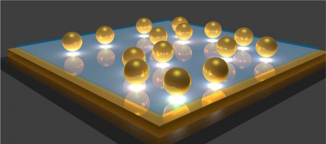
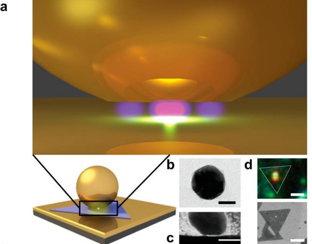
These nanocavities are created in a very simple way. Instead of two nanoparticles, so-called nanoparticle dimers, and trying to place a semiconductor material between them, the team uses a gold surface, smooth as a mirror, cover it with a few layers of a 2D semiconductor and then place nanoparticles on top (see Figure 1). If we imagine these nanoparticles as spheres, the contact with the semiconductor would be ideally a point or, in reality, a facet, thus creating stable and well-defined junctions with intriguing materials properties. This geometry is aptly called nanoparticle on mirror (NPoM).
When a nanoparticle close to a metallic surface is illuminated, an optical scattering spectrum appears consisting of several coupled modes. Some of these modes correspond to the nanoparticle alone, but the dominant ones are because of the coupling between the nanoparticle and “its image” in the mirror surface. The spectral positions of these modes reveal the morphology of the cavity created between the nanoparticle and the mirror and are highly sensitive to small variations of the nanoparticle facet sizes. In other words, the NPoM forms a metal-insulator-metal cavity with lateral boundary conditions defined by the facet width.
The researchers investigated two kinds of 100 nm gold NPoMs. In one of them the semiconductor spacer was a four-atom-layer thick cadmium selenide (CdSe). CdSe creates 1.4 nm thick gaps and, when irradiated, undergoes photochemical oxidation which enables a direct real-time study of the response to variations of the dielectric environment inside the gap. In the other, a monolayer of molybdenum disulphide (MoS2) creates 0.65 nm gaps, but it is chemically stable when illuminated and, in contrast with graphene, is intrinsically insulating.
When the NPoMs are illuminated, the researchers found that the modes in the resulting spectrum suffer a shift over time that depends on the spacer composition. In the case of MoS2 the modes move slowly, apparently depending on the exact morphology of the cavity. With CdSe the researchers find that the slow shift is accompanied by an initial much faster one.
These shifts imply that something changes within the cavities. The slow redshifts common to both systems are explained by nanoscale resculpting of the gold atoms around the junction region. For example, a 1% shift in the j2 mode corresponds to a change in the facet radius of less than 1 atom. The fast redshift arises from a fast photochemical reaction that turns CdSe into CdO in the surface layer.
The authors demonstrate that optics provides an exquisitely sensitive tool to track material dynamics at the nanoscale. To picture it, consider that this methodology is already sensitive to 10 gold atoms adhering to a facet each 10 milliseconds. And this can be further optimized.
Apart from the study of material modifications in extremely confined volumes (corrosion, catalysis, etc.), the fact that atoms are mobile under optical irradiation is critically relevant for the new developments in heat-assisted magnetic recording (HAMR) for hard-drives, a favoured industrial solution to high density data storage. Something that only a Feynman could have imagined.
Author: César Tomé López is a science writer and the editor of Mapping Ignorance.
References
- Daniel O. Sigle, Jan Mertens, Lars O. Herrmann, Richard W. Bowman, Sandrine Ithurria, Benoit Dubertret, Yumeng Shi, Hui Ying Yang, Christos Tserkezis, Javier Aizpurua, and Jeremy J. Baumberg (2015) Monitoring Morphological Changes in 2D Monolayer Semiconductors Using Atom-Thick Plasmonic Nanocavities ACS Nano DOI: 10.1021/nn5064198 ↩