Semiconductor devices: photoconductivity
Semiconductor devices: photoconductivity

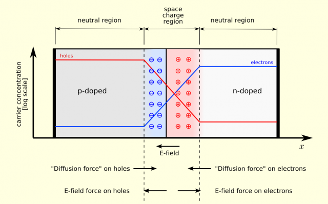
Let’s take a p-type semiconductor with a very clean surface and place it right next to the clean surface of a n-type semiconductor. This type of device is called an n-p junction diode, or simply a diode. What happens? Scientists realized that the electrons in the conduction band of the n-type semiconductor are able to move across the boundary between the two semiconductors, and fall into the holes in the lower energy valence band of the p-type semiconductor. The electrons and holes begin to disappear. But as the electrons disappear in the n-type, the positive charges of the impurities are no longer balanced by the negative conducting electrons, so the n-type becomes positively charged. The opposite happens in the p-type semiconductor.
As the holes disappear, the impurities are left holding an extra electron, which causes the p-side to become negatively charged. The result of all this is that after a very short time a net electric field is set up between the n-type and p-type semiconductors which stops the process of mutual destruction by keeping the electrons on the n-type side separated from the holes on the p-type side, with a “depletion layer” in the middle.
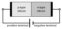
Now, if a potential difference, such as one caused by a small battery, is placed across the device from the p-type side to the n-type side, the equilibrium may or may not be disturbed, depending upon how the potential is placed. If the positive wire is placed on the n-type material and the negative wire on the p-type material, the separation of the electrons and holes is reinforced. So no current will flow. But, if the wires are reversed, so that the positive wire is placed on the p-type material and the negative wire on the n-type side as in Figure 2, the negative electrons on the n-type side will be pushed toward the boundary, and the same for the positive holes on the p-type side. If the external potential is greater than the internal potential of these two, a current will flow in the device.
The current will be enhanced if now a photon arrives from the outside and pushes an electron from the n-type material into the conduction band. The n-p diode can then be used as an even more powerful photocell than a simple semiconductor alone. Perhaps the most common use of this type of photocell is in the generation of electricity from solar energy. This can be done for small-scale devices, such as pocket calculators, or for larger scale energy needs, such as the energy for an entire building. Such photocells are often known as photovoltaic cells. The International Space Station and other satellites near the earth’s orbit depend for their energy needs upon huge “wings” of photovoltaic cells, unfurled to catch the radiation from the sun.
Research continues on how to make even greater use of photoconductivity from the sun’s rays to produce electrical energy for our needs on a large scale. The DIPC is at the forefront of this effort.
Author: César Tomé López is a science writer and the editor of Mapping Ignorance.