B-graphene: from large scale to local environment
B-graphene: from large scale to local environment
The current in a semiconductor consists of two parts: the negatively charged electrons in the conduction band and the positively charged holes in the valence band. Although the number of electrons in the conduction band is equal to the number of holes in the valence band, the two contributions to the current are in general not equal, because the electrons in the conduction band move more easily than the electrons in the valence band. Typically, the contribution of the electrons to the current at room temperature is about two to four times the contribution of the holes.
Because only 1 electron in 109 contributes to the conductivity of an intrinsic semiconductor, the presence of impurities can significantly alter the conductivity of the semiconductor in a way that might not be easily controllable. However, if impurities with known properties are deliberately introduced into the semiconductor in carefully controlled amounts, their contribution to the conductivity can be precisely determined. At impurity levels of only 1 part in 106 or 107, the impurity contribution to the conductivity dominates the intrinsic contribution. Such materials are known as impurity semiconductors, and the process of introducing the impurity is known as doping. Impurity semiconductors can be of two varieties: those in which the impurity contributes additional electrons to the conduction band and those in which the impurity contributes additional holes to the valence band.
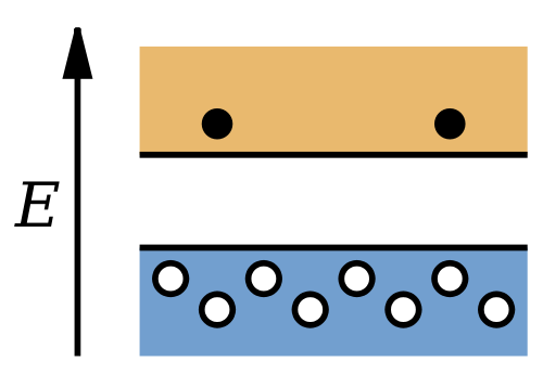
A semiconductor that has been doped with donor impurities is known as an n-type semiconductor, because the conductivity is due mostly to the negative electrons. A material that has been doped with acceptor impurities is known as a p-type semiconductor, because the conductivity is due mostly to the positively charged holes.
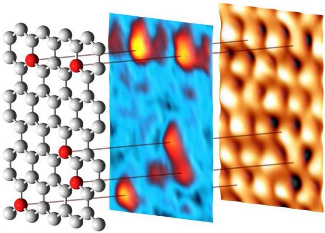
By substituting carbon atoms with nitrogen or boron, it is possible to turn graphene into a semiconductor of n- or p-type, respectively. The modifications of the electronic structure induced by the impurities greatly increase the possibilities of using doped graphene in nanoelectronics, in oxygen reduction reactions occurring in fuel cells, batteries, supercapacitors and many other applications. As compared to nitrogen, boron can be embedded in graphene at higher concentrations that give broader opportunities to tune its properties. This makes boron-doped graphene (B-graphene) a unique and very attractive material from both the fundamental and the practical viewpoints. We know that the structure of B-graphene is governed by the synthesis method and conditions, and postgrowth treatment as well, but currently it is not well-known.
Now a group of researchers, that includes Mikhail Otrokov, Andrés Arnau, Evgueni Chulkov from Materials Physics Center CSIC-UPV/EHU and DIPC, coordinated by Ikerbasque’s Denis Vyalikh, currently at Dresden University of Technology but joining DIPC next year, has presented1 in ACSNano a comprehensive study of the structural organization, from large scale to local environment of foreign atoms, of B-graphene.
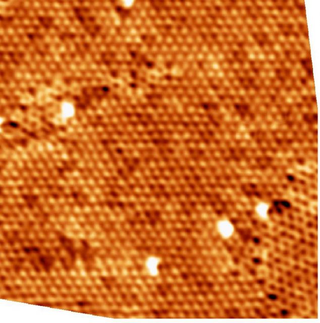
The researchers used a method which has become key for large-scale graphene growth on a wide variety of substrates, chemical vapour deposition, to grow single-layer B-graphene from carborane molecules on Ni (111) and Co(0001). The used a broad variety of surface-sensitive methods to study the structure of boron impurities during the synthesis.
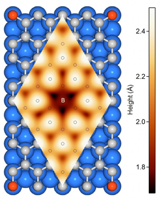
The results confirm that the impurities do substitute carbon atoms in the graphene lattice, thus affecting the orientation of graphene domains. One important conclusion is that it is possible to substitute up to 19% of the carbon atoms with boron using this method. There is one caveat, though. B-graphene on the Co(0001) surface may be grown better oriented on the large scale for boron concentrations up to 15 %; still its honeycomb lattice is strongly distorted on atomic scale, similarly to what happens with the B-graphene/Ni(111). It is at low concentrations (< 5%) that B-graphene is well-oriented on Ni(111).
These results represent an important step towards the knowledge of the behaviour of doped graphene, which may help find applications of graphene in the next generation of electronic devices.
Author: César Tomé López is a science writer and the editor of Mapping Ignorance.
References
- Dmitry Yu. Usachov, Alexander V. Fedorov, Anatoly E. Petukhov, Oleg Yu. Vilkov, Artem G. Rybkin, Mikhail M. Otrokov, Andrés Arnau, Evgueni V. Chulkov, Lada V. Yashina, Mani Farjam, Vera K. Adamchuk, Boris V. Senkovskiy, Clemens Laubschat, and Denis V. Vyalikh (2015) Epitaxial B-Graphene: Large-Scale Growth and Atomic Structure ACS Nano DOI: 10.1021/acsnano.5b02322 ↩