Graphene band gap engineering using boron
Graphene band gap engineering using boron

Among the astonishing properties of graphene, a high mobility of the charge carriers has placed this material into the focus of intensive research efforts, aimed at developing high-speed graphene-based electronic devices. The first device of this family, a graphene field-effect transistor (GFET), still remains a promising candidate for applications in flexible electronic circuits.
An essential handicap that limits the performance of planar GFETs is the absence of a band gap in the graphene electronic structure. The gap is necessary to reach a high on/off current ratio. In the recent past, several approaches have been developed for opening and controlling the gap. These methods include adsorption of atoms and molecules, but the material still remains gapless.
A promising approach for the graphene band gap engineering is to introduce a large-scale sublattice asymmetry. When the foreign atoms become randomly embedded only in one graphene sublattice, the resulting system possesses a notable band gap improving the transport properties of conventional GFETs. Experimental observation of the discussed unbalanced sublattice doping is quite elusive, though. Doping asymmetry was detected with scanning tunneling microscopy (STM) in nitrogen-doped graphene, grown on a Cu(111) substrate. It was proposed that a possible mechanism responsible for breaking of the sublattice symmetry is related to oscillations in the local density of states driven by the impurities.
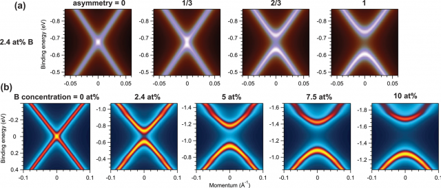
Now an international team of researchers, that includes Mikhail M. Otrokov, Evgueni V. Chulkov and Ikerbasque professor Denis V. Vyalikh from DIPC, using photoelectron diffraction and spectroscopy has demonstrated1 a selective incorporation of boron impurities into only one of the two graphene sublattices. Such boron-doped graphene possesses a band gap that can be precisely controlled by the dopant concentration. B-graphene with doping asymmetry is, thus, a novel material, which is worth considering as a good candidate for electronic applications.

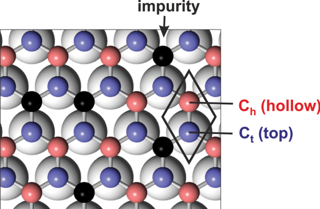
The approach is illustrated in Figure 1. When doped graphene is synthesized on a crystal face with hexagonal structure and well-matched lattice constant, a strong symmetry breaking may occur. This happens when one sublattice, marked as Ct, is adsorbed on top of the substrate atoms of Co(0001), while the other sublattice Ch occupies the hollow sites.
The early studies of the graphene/Co(0001) system showed that graphene is formed by randomly oriented domains sticked to the metallic substrate. However, it was recently shown that under certain conditions well-oriented graphene can be grown. Such an interface, and particularly its geometry, remain poorly explored, though. In the present work, the researchers unveil the structural properties of the graphene/Co(0001) interface and show that the cobalt substrate is very well suitable for large-scale unbalanced doping of graphene with substitutional boron impurities.
In the well-oriented graphene/Co(0001) system, one sublattice of carbon is placed above Co atoms, while the second one occupies the hollow sites. This unique property of the interface makes cobalt an ideal substrate to be used as a platform for the synthesis of doped graphene with impurities incorporated in one of the two C-sublattices. This is conclusively demonstrated by the example of the B-graphene/Co(0001) system, in which boron impurities preferably substitute carbon atoms in one sublattice, located above the hollow sites of the metal substrate.
The ab initio calculations predict that such asymmetrically doped graphene should have an intrinsic band gap and the width of the gap can be controlled by the dopant concentration. Thus, B-graphene with demonstrated doping asymmetry becomes a novel material, which is worth considering as a good candidate for applications in GFETs and other graphene-based electronics.
Author: César Tomé López is a science writer and the editor of Mapping Ignorance
References
- Dmitry Yu. Usachov, Alexander V. Fedorov, Oleg Yu. Vilkov, Anatoly E. Petukhov, Artem G. Rybkin, Arthur Ernst, Mikhail M. Otrokov, Evgueni V. Chulkov, Ilya I. Ogorodnikov, Mikhail V. Kuznetsov, Lada V. Yashina, Elmar Yu. Kataev, Anna V. Erofeevskaya, Vladimir Yu. Voroshnin, Vera K. Adamchuk, Clemens Laubschat, and Denis V. Vyalikh (2016) Large-Scale Sublattice Asymmetry in Pure and Boron-Doped Graphene Nano Letters doi: 10.1021/acs.nanolett.6b01795 ↩