How to create a band gap in graphene using lead
How to create a band gap in graphene using lead

Graphene is one of the most promising materials for nanoelectronics owing to its unique Dirac cone-like dispersion of the electronic state and high mobility of the charge carriers. We all know that already, provided we are a little bit interested in condensed matter physics. But the point is that, in order to facilitate the implementation of a graphene-based device, an essential change of the electronic structure of graphene must be achieved first – namely, the controlled creation of a band gap. Two fundamentally different mechanisms are known to be able to do just that: a sublattice symmetry breaking or an induced strong spin−orbit interaction. The band gap appearance can drive graphene into a narrow-gap semiconductor if we use the first, or into a 2D topological insulator phase if we use the second. Both cases are technologically relevant.
From the point of view of the Earth we can consider that the Sun revolves around it if that suits us for some calculation. The same way, the nucleus of an atom would orbit an electron. It happens that the nucleus has a positive charge, and we know that a moving charge originates a magnetic field. As the electron has an intrinsic magnetic moment (spin) there must be a magnetic interaction between the spin of the electron and the magnetic field due to the orbit of the nucleus. This is what is known as spin-orbit effect.
In graphene the spin-orbit effect is negligible, because we are considering carbon atoms, where relativistic effects are very small. This is because the speed of electrons are relatively small as well. Relativistic effects, and stronger spin-orbit interactions, are usually found in heavier elements.
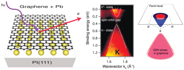
Now, a team or researchers, including Evgueni V. Chulkov from DIPC and CFM, has used 1 angle-resolved photoemission spectroscopy (ARPES) to study the electronic and spin structure of graphene on Pt(111) intercalated by a full Pb monolayer. By employing a low energy electron diffraction (LEED) technique, they show that an intrinsic spin−orbit coupling appears in graphene and leads to an opening of a wide band gap between its valence and conduction bands.
The researchers show the graphene lattice to be commensurate with that of the underlying Pb/Pt(111) substrate, characterized by the formation of the ordered Pb c(4 × 2) superstructure. It is this commensurability what favors the enhancement of an intrinsic spin−orbit coupling in graphene.
This work builds on that of Calleja et al (2014) where it was shown that, for graphene on Ir(111) with one atom thick Pb island intercalated in between, the Pb interlayer induces a strong spin-orbit interaction in graphene that is spatially modulated near the Pb island edges, acting as a pseudomagnetic field. But no photoemission studies of the electronic and spin structure of graphene contacted with Pb had been reported so far, and the experimental realization of the spin−orbit gap in graphene system was still a pending problem.
This new work comes to experimentally demonstrate the spin−orbit gap opening in the Dirac point of graphene contacted with the lead interlayer. As a result, the analysis of the system’s low energy spectrum has revealed a gap of about 200 meV, separating the graphene π states. According to previous theoretical predictions, such a band structure corresponds to enhancement of the intrinsic spin−orbit interaction in graphene that results in the spin−orbit gap formation and satisfies the conditions of the quantum spin Hall phase onset.
Author: César Tomé López is a science writer and the editor of Mapping Ignorance.
References
- Ilya I. Klimovskikh, Mikhail M. Otrokov, Vladimir Yu. Voroshnin, Daria Sostina, Luca Petaccia, Giovanni Di Santo, Sangeeta Thakur, Evgueni V. Chulkov, and Alexander M. Shiki (2017) ACS Nano doi: 10.1021/acsnano.6b05982 ↩
1 comment
[…] Lo del grafeno está muy bien y tiene muchas posibilidades y tal. Pero lo cierto es que hay que modificarlo para que funcione en un dispositivo real. Y la gente del DIPC está haciendo avances en precisamente eso: How […]