Identifying the bottlenecks for improving quantum-dot based devices
Identifying the bottlenecks for improving quantum-dot based devices
Minimizing losses in any kind of electronic device is always important, but it is paramount in nanoelectronics. Still, most of the phenomena that lead to inefficiencies in the operation of these nanodevices are poorly understood.
Consider the case of quantum dots. A quantum dot is a nanometric crystalline structure of semiconductor materials. In a quantum dot, electrons are confined in a region of space, thus creating a well-defined structure of energy levels that depends very much on the size and shape of the quantum dot. In quantum dot based devices such as solar cells, LEDs, and thermoelectrics a major limitation to the efficiency is charge trapping.
In devices made of crystalline bulk materials, the most common trapping sites are impurities or defects of the crystal structure such as vacancies or interstitial atoms. However, in multi- and nanocrystalline materials, surface defects play a dominant role. In cadmium telluride (CdTe) solar cells, for example, grain boundaries were identified as the major defect site. Therefore, in order to reduce losses some strategies are possible: grain growth (i.e., diminishing the number of grain boundaries) and electronic passivation using some chloride salts, among them.
But in the case of quantum-dot based devices, surface defects are even more important as the surface area is very high. As a result, a lot of experimental research has been done that has provided a repertoire of recipes for electronic passivation, using inorganic shells or ligand exchange, but few, and mostly theoretical, studies have been done to address the nature of the physical and chemical processes responsible for trapping. In short, the exact nature of the involved surface traps remains poorly understood.
Now, a group of researchers that include Jon Mikel Azpiroz and Ivan Infante from the Kimika Facultatea UPV/EHU and DIPC, has focused1 on a quantum-dot cadmium telluride solid to investigate both experimentally and theoretically the trapping mechanism and the kind of chemical reaction at play during charge trapping in the quantum dots. Their results are published in Nano Letters.
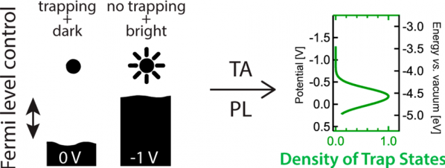
The researchers report the first experimental determination of the density of trap states of a film of cadmium telluride quantum dots, using a novel combination of electrochemistry and ultrafast spectroscopy. When traps are empty, electron trapping proceeds on a (sub-)picosecond time scale; when traps are filled electrochemically, this process takes nanoseconds. They find a density of trap states close to the valence band. The theoretical calculations done using density functional theory are consistent with this finding and assign it to dicoordinated tellurium atoms at the quantum dot surface as a result of a loss of ligands during the film processing.
Time-resolved photoluminescence experiments reveal that hole trapping also occurs, albeit at least one order of magnitude slower than electron trapping. The slower hole trapping and the fast capture of electrons by traps close to the valence band can be explained by an Auger-mediated trapping mechanism.
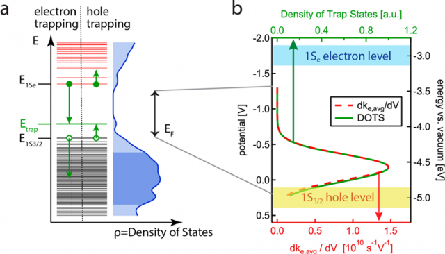
This Auger-mediated trapping is shown schematically in Figure 2. This process involves the trapping of the electron (hole) by scattering with the geminate hole (electron). The energy difference in the trapping process is not dissipated to phonons but is given to the second charge carrier, which subsequently cools down to the band edge. The Auger process permits large energy losses for the electron in the trapping process. If the matrix elements for electron and hole Auger-mediated trapping do not differ too much, the result will be that the Auger trapping rate is much higher for electrons than for holes. Thus, explaining the observed order of magnitude difference in electron and hole trapping rates.
In all, the researchers are able to assign a density of trapping states to the exact composition and geometry of the surface using a unique combination of experimental and theoretical approaches, identifying the bottlenecks for improving quantum-dot based devices.
Author: César Tomé López is a science writer and the editor of Mapping Ignorance.
References
- Simon C. Boehme, Jon Mikel Azpiroz, Yaroslav V. Aulin, Ferdinand C. Grozema, Daniël Vanmaekelbergh, Laurens D.A. Siebbeles, Ivan Infante, and Arjan J. Houtepen (2015) Density of Trap States and Auger-mediated Electron Trapping in CdTe Quantum-Dot Solids Nano Letters DOI: 10.1021/acs.nanolett.5b00050 ↩
1 comment
[…] Identifying the bottlenecks for improving quantum-dot based devices […]