How to phase-engineer Josephson topological materials
How to phase-engineer Josephson topological materials
When we approximate two superconducting materials at low temperature, so that they are only separated by a very thin layer (less than 10 nanometres thick) of an insulating material, some new and very interesting electrical effects can be observed.
If normal conducting metals are separated by such a barrier in that conditions it is possible for a small current to flow between the conductors by the tunnel effect, a typical quantum mechanical phenomenon.
But if the materials are superconductors some unusual phenomena occur. First, a supercurrent, a current with zero resistance, that is, can flow through the barrier. If this current exceeds a critical value, this conductivity is lost; the barrier then only allows the small current flow due to the tunnel effect and a voltage develops across the junction. If we apply a magnetic field below the critical current value we will find that the net current through the barrier depends on the magnetic field that we are applying. If the field increases beyond a critical value the supercurrent vanishes.
A junction like the one we have just described is called a Josephson junction; two or more of them joined by superconducting paths is called a Josephson interferometer. These junctions can be used in measuring fundamental constants, in defining a voltage standard or to measure magnetic fields accurately. An important potential use is in logic components in high-speed computers. Josephson junctions can switch states very quickly (as low as 6 picoseconds). Moreover, they have very low power consumption and can be packed closely without generating too much heat.
But, what if instead of an insulating material we use a conducting metal in a Josephson junction? In this case superconducting correlations are induced in the normal metal due to the proximity effect. At the interface between a normal conductor and a superconductor, charge is transferred from the normal conductor to the superconductor. This results in the formation of a Cooper pair in the superconductor and a reflected hole in the normal conductor. This phenomenon is called an Andreev reflection.
As a consequence of these reflections, the normal metal acquires genuine superconducting-like properties such as the ability to sustain a supercurrent and a gap in the density of states (DOS), the amplitude of which can be controlled by the macroscopic phase difference between the superconducting leads. This process therefore enables the normal metal to possess a character that ranges from insulator-like (gapped state) to conductor-like (gapless state).
On the other hand, nothing forbids that a Josephson junction could be formed by more than two leads. Actually, two-terminal Josephson junctions based on the proximity effect have been the focus of intense research for several years, and only recently three-terminal junctions have been built to investigate the physics of the multiple crossed Andreev reflections that exist in metallic weak links.
Yet the impact and control of three superconducting phases acting on a nanosized normal metal have not been explored so far, despite recent predictions that multi-terminal Josephson junctions could be used to tailor and control exotic quantum states: from spin qubits to the spooky Majorana bound states of topological superconductors.
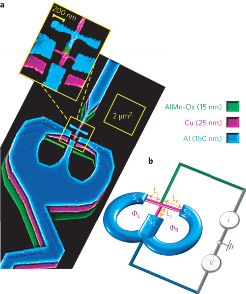
Now, a team of researchers, including F. Sebastian Bergeret, from MPC (CSIC-UPV/EHU) and DIPC, report 1 the realization of a phase-tunable three-terminal Josephson junction interferometer based on the proximity effect in a diffusive metallic island, called omega-shape superconducting quantum interference proximity transistor (ω-SQUIPT) due to its characteristic shape.

The device consists of three different parts, as shown in Figure 1a. Aluminum is used to form the superconducting double-ring structure that consists of three leads converging into a nanosized T-shaped copper weak link.
Two different families of ω-SQUIPTs were fabricated and characterized: an A-type interferometer (shown in Fig. 1a), and a B-type interferometer, which is less symmetric with respect to the length of the arms that form the T-shaped region and to the resistances of the three Cu/Al interfaces. These two families of interferometers allow different topologies of the electron states in the weak link to be accessed by tuning the external magnetic flux.
The tunnelling spectroscopy measurements performed reveal transitions between gapped (insulating) and gapless (conducting) states that are controlled by the phase configuration of the three superconducting leads connected to the junction.
The gapless regions are the domains where the zero-energy singularities at the individual state level are supposed to occur: Weyl singularities or, at a sufficiently strong spin–orbit coupling, the zero-energy crossings that signal the transitions between different parities or the emergence of Majorana bound states. The ω-SQUIPT could therefore easily be combined with hybrid nanocircuits based on semiconducting nanowires, low-dimensional systems, graphene or superconductors, for example, to enhance its functionalities. In other words, the observation of the gapless state is pivotal for enabling phase engineering of different and more sophisticated artificial topological materials.
Author: César Tomé López is a science writer and the editor of Mapping Ignorance
References
- E. Strambini, S. D’Ambrosio, F. Vischi, F. S. Bergeret, Yu. V. Nazarov and F. Giazotto (2016) The ω-SQUIPT as a tool to phase-engineer Josephson topological materials Nature Nanotechnology doi: 10.1038/nnano.2016.157 ↩