How to synthesize a nanoporous graphene that is both transistor and molecular sieve
How to synthesize a nanoporous graphene that is both transistor and molecular sieve

Graphene is a two-dimensional allotrope of carbon made of hexagons. It is a zero-gap semimetal with a tiny overlap between valence and conductance bands. Since the isolation of graphene in 2004, considerable interest has been paid to exploring its applications in a variety of fields such as electronics, composites, sensors, catalysis and energy related systems. But, in order to facilitate the implementation of a graphene-based device, an essential change of the electronic structure of graphene must be achieved first – namely, the controlled creation of a band gap.
Two fundamentally different mechanisms are known to be able to do just that: a sublattice symmetry breaking or an induced strong spin−orbit interaction. The band gap appearance can drive graphene into a narrow-gap semiconductor if we use the first.
Processing graphene into nanoribbons – strips of graphene – with widths of less than 10 nm can open up a band gap that is sufficient for room temperature field effect transistor applications. Unfortunately, graphene nanoribbon-based devices often have low driving currents, making them unsuitable for practical applications.
Enter nanoporous graphene (NPG), a unique graphene nanostructure that can be regarded as a densely interconnected network of multiple nanoribbons Through the formation of NPGs it is possible to open an energy band gap in a large area graphene sheet to generate a semiconducting thin carbon film.
But NPG could be much more than a transistor component. It also has potential applications as an atom-thick selective nanosieve for sequencing, ion transport, gas separation, and water purification.
Now, we can consider the possibility of having it all combined: a semiconductor behaviour in a molecular sieve. It is not that easy, though. Selectivity in molecular sieving is achieved by reducing the pore size to the scale of single molecules. When this has been achieved, graphene remains semimetallic. Similarly, inducing semiconducting gaps for room temperature gate actuation requires, as we mentioned above, the generation of sub-10 nanometer ribbons between pores. In this range, atomic scale disorder and width fluctuations have substantial impact on gap uniformity. Hence, combining semiconducting and sieving functionalities in a single nanoporous graphene material is a challenging task that requires the simultaneous generation of nanometer size pores and ribbons that have to be carved with atomic precision.
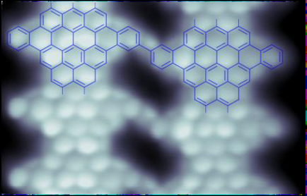
And a method to achieve precisely this is what a team of researchers, with the participation of DIPC’s Bernhard Krentz and Iberbasque’s research associate Arantzazu Garcia Leuke, has just published 1 in Science: a bottom-up method to synthesize atomically-precise nanoporous graphene that combines transistor with molecular sensing and sieving functionalities.

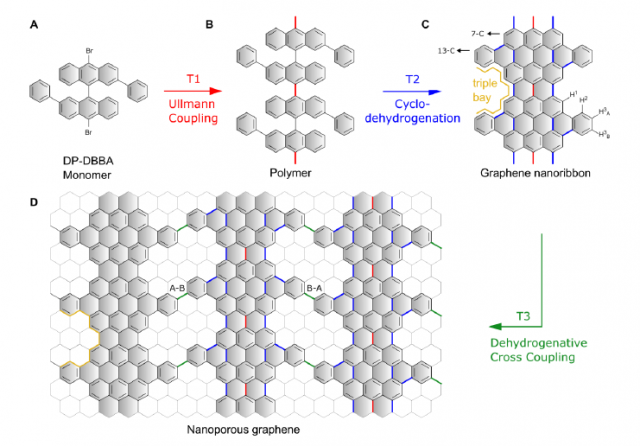
The method relies on the hierarchical control of three thermally activated reaction steps, labelled as T1-T3 in Figure 1. Nanoribbons and pores with nanometer size, atomic-scale uniformity and long-range order are formed in separate steps. Graphene nanoribbons are first synthesized by following a known route, consisting on the surface-assisted Ullmann coupling of aromatic dihalide monomers into polymer chains (T1), and the cyclodehydrogenative aromatization of the intermediate polymeric chains into nanoribbons (T2). The final step (T3) interconnects nanoribbons laterally in a reproducible manner via a highly selective dehydrogenative cross coupling. The size, density, morphology and chemical composition of the pores are defined with atomic precision by the design of the molecular precursors.
Measurements reveal a highly anisotropic electronic structure, where orthogonal one-dimensional electronic bands with an energy gap of aproximately 1 eV coexist with confined pore states, making the nanoporous graphene a highly versatile semiconductor for simultaneous sieving and electrical sensing of molecular species.
Author: César Tomé López is a science writer and the editor of Mapping Ignorance
References
- César Moreno, Manuel Vilas-Varela, Bernhard Kretz, Aran Garcia-Lekue, Marius V. Costache, Marcos Paradinas, Mirco Panighel, Gustavo Ceballos, Sergio O. Valenzuela, Diego Peña, and Aitor Mugarza (2018) Bottom up synthesis of multifunctional nanoporous graphene Science doi: 10.1126/science.aar2009 ↩
3 comments
A experimental research, 3 centers, and you only mention… just the theoretical ones!!!
Well, in just one line you justify what you criticize: apparently, you did not see in what you label as “experimental research” the “theoretical contribution”.
In any case, I tend to present the framework necessary, as I see fit, for the comprehension of what has been discovered. For a whole treatment of the subject, with all the experimental and theoretical hows, and a full list of the institutions involved you may find the technical article duly linked. Finally, as this is DIPC’s channel I just mention that there is a contribution from DIPC. For politically conscious texts you can refer to those issued by the official communication centres, assuming those texts exist.
Probably my short sentence can be improved, but the message was pretty clear. Obviously, as anyone who knows research, it is really far from my intention undermine the relevance of any theoretical work. And also obviously, in this achievement the experimental part is highly relevant.
Thus, in my opinion, a divulgation article which mentions the authors it should include at least all the relevant teams and/or institutions. I did not know mappingignorance.com is a DIPC’s channel, but it does not change my view. Since you mention it, a joint press release was issued, as well as a joint press conference.
Having said that, I should like to point it was a good article and we need this kind of quality divulgation media.