Hexagonal boron nitride monolayer films can be successfully grown on a curved Ni(1 1 1) substrate
Hexagonal boron nitride monolayer films can be successfully grown on a curved Ni(1 1 1) substrate
Since the discovery of graphene, a wide diversity of atomic-layer-thick, two-dimensional (2D) materials with varied properties have emerged. Of particular interest are those that exhibit semiconducting behavior, such as hexagonal boron nitride (hBN). hBN is isoelectronic to graphene and has also a honeycomb lattice formed by alternating nitrogen and boron atoms, but in contrast to the semi-metallic graphene, its band structure presents some characteristics that makes it particularly attractive for applications in microelectronics, either alone or in combination with other 2D materials, such as graphene.
In top of that hBN is structurally robust and chemically inert, properties that are particularly relevant for coating and hydrogen storage applications.
For all these reasons, as you can imagine, there exists an increasing demand for large size hBN films that can be transferred to different surfaces. The problem is that first you need these films to be synthesized on adequate substrates by different growth techniques. Hence, the increasing interest on single-layer hBN, doped and intercalated hBN/metal interfaces, and low-dimensional hBN structures, such as nanoribbons, has prompted the search of appropriate substrates, in order to achieve functional hBN layers and nanostripes with abrupt interfaces.
The growth challenge for hBN is similar to the one faced by other hetero-epitaxial systems in the past, what makes the experience acquired over decades, particularly about the balance and hierarchy of driving forces that govern crystal growth extremely handy. Among these driving forces we find atomic lattice matching, which is often sought to prevent large accumulation of stress in extended films, and nanotemplating, as a way to optimize growth by altering energetics and kinetics. In this context, stepped (or vicinal) surfaces emerge as simple self-organized growth templates, known to facilitate the synthesis of one-dimensional nanostructures, such as atomic rows and nanostripes and to promote single rotational domains in growing films.
Despite the advantages and versatility of vicinal surfaces as growth templates, very little has been done in regards to 2D, monolayer-thick materials. One obvious reason is the added structural complexity of the stepped interface. Additionally, vicinal surfaces are not rigid frames that remain static or passive during epitaxy, but, on the contrary, they often respond to overlayer growth by step-edge roughening, step bunching or nano- and mesoscale faceting. All these possibilities are difficult to predict and, given the infinite variety of vicinal planes to each high symmetry orientation, their practical understanding can gain from systematic investigations using curved surfaces.
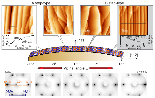
In this context, it has recently been shown that a very facile, and hence effective implementation of the curved surface approach is achieved with cylindrical sections of single crystals, such as the one sketched in figure 1. This represents a portion of a cylindrical Ni single crystal in which almost the entire family of Ni(1 1 1) vicinal planes with A-type ({1 0 0} microfacet) and B-type ({1 1 1} microfacet) close-packed steps are found at both sides of the (1 1 1) center, up to the (3 3 5) and (2 2 1) crystal directions, respectively.
Now, an international team that includes researchers from DIPC, CFM and UPV/EHU, have thoroughly explored 1 the synthesis of a single layer hBN on vicinal Ni(1 1 1) surfaces with close-packed steps using the curved sample [in short, c-Ni(1 1 1)] described in figure 1. The c-Ni(1 1 1) crystal has the advantage of having the Ni(1 1 1) surface at the center of the sample, and hence they could use the well-studied hBN/Ni(1 1 1) interface as a reference. Previous studies using Ni foils with differently oriented grains already suggested different growth scenarios.
Beyond Ni, the synthesis of the hBN monolayer has been investigated for many high-symmetry metal surfaces. It is generally observed that electronic and structural properties of the epitaxial hBN monolayer are influenced by both the strength of the interface chemical bond and the registry, that is, the lattice-matching with the substrate. At close-packed surfaces, the interaction varies from strong hBN chemisorption on Ni(1 1 1), Co(0 0 0 1), Rh(1 1 1), Ru(0 0 0 1) and Ir(1 1 1), to weak interaction on quasi-noble Pd [50] and Pt, and noble Cu(1 1 1) and Ag(1 1 1) surfaces.
Experiments at (1 1 0) surfaces of Ni, Fe, Cr, Cu, Pd, and Mo reveal the little influence of the crystal orientation on the hBN/metal interaction strength. With respect to the hBN layer structure, the relevant feature is the presence of a characteristic nanoscale corrugation, called ‘nanomesh’, in strongly interacting interfaces with poor lattice matching, whereas nearly flat hBN films are observed otherwise. The latter is the case of Ni(1 1 1).
The experiments on the c-Ni(1 1 1) curved sample reveal homogenous coating of the Ni substrate, although step-bunching and faceting at all Ni(1 1 1) vicinal planes. In the A step-type side of the crystal, a two-phase,hill-and-valley structure is observed, driven by the excellent registry of hBN with flat Ni(1 1 1) terraces (first phase) and with the stepped Ni(1 1 5) plane (second phase). In the B step-type side, Ni(1 1 1) terraces are also present, but the lack of reasonably matched B-type vicinal planes explains the presence of the incommensurate (5.15 × 1) hBN/Ni(1 1 0) facet, for which a minimum expansion/contraction of the rigid hBN lattice is required.
All spectroscopic data in faceted regions are explained by the incoherent superposition of the signal from the (1 1 1) terrace and the faceted phase. A direct comparison is then possible of the strength of chemical interactions and other electronic properties, such as the valence band maximum, among the three hBN-covered Ni(1 1 1), Ni(1 1 5) and Ni(1 1 0) interfaces. The differences found are consistent with the variable atomic-scale roughness at each interface, from the flat and sharp hBN/Ni(1 1 1), to the rough, stepped (1 1 5) substrate, and to the corrugated hBN layer on Ni(1 1 0).
As a conlusion the researchers find that hBN monolayer films can be successfully grown on a curved Ni(1 1 1) substrate . The results suggest the use of Ni(1 1 5) and vicinal Ni(1 1 0) surface to achieve homogenous, monolayer thick hBN with weaker coupling with the Ni ferromagnetic substrate.
Author: César Tomé López is a science writer and the editor of Mapping Ignorance
References
- L Fernandez, A A Makarova, C Laubschat, D V Vyalikh, D Yu Usachov, J E Ortega and F Schiller (2019) Boron nitride monolayer growth on vicinal Ni(1 1 1) surfaces systematically studied with a curved crystal 2D Mater. doi: 10.1088/2053-1583/ab01e7 ↩