Engineering high Chern number materials
Engineering high Chern number materials
Some materials have special universal properties protected against perturbations. Such properties are theoretically described by topology, a branch of mathematics concerned with the properties of geometrical objects that are unchanged by continuous deformations. So-called topological insulators are electronic materials that have a bulk band gap like an ordinary insulator but have conducting states on their boundaries, i.e., edges or surfaces. The conducting surface is not what makes topological insulators unique, but the fact that it is protected due to the combination of spin-orbit interactions and time-reversal symmetry.
A topological invariant is a geometrical quantity that remains unchanged by continuous deformations. Topological invariants have found widespread applications in physics, chemistry, and materials science. One of the best known topological invariants in condensed matter physics is the Chern number.
The definition of the Chern number is not exactly simple. But it could be enough to understand the Chern number as an integer that characterizes the topology of filled bands in two-dimensional lattice systems. A band with a non-zero Chern number is topologically non-trivial. When the highest occupied band is non-trivial and completely filled, the state is called a topological insulator. A material whose topological phases can be characterized by the Chern number is called a Chern insulator, a class of topological insulators. In other words, a Chern insulator state is a quantum phase of two-dimensional gapped materials with broken time-reversal invariance and nontrivial electronic band topology.
The edge modes of a Chern insulator conduct electricity without dissipation, which could be useful for the construction of novel highly efficient chiral interconnects for low-power-consumption electronics. However, the contact resistance between a metal electrode and a Chern insulator in these devices may limit their performance. To reduce this resistance as much as possible, the number of chiral edge modes, i.e., the Chern number C, should be as large as possible. Therefore, it is of great interest and importance to engineer Chern insulators with high Chern numbers.
The Chern insulator state was first observed in 2D electron gases in 1980 in a transport phenomenon that is now known as the quantum Hall effect. Imagine that we have a conductor or a semiconductor through which a current is flowing. Then we apply a strong transverse magnetic field. As a result, we can measure a potential difference at right angles to both the current and the field caused by the deflection of charge carriers by the field. This effect was described by Edwin Hall in 1879 and is the classical Hall effect. . It introduces a coefficient, RH, a constant characteristic of the material. A quantum mechanical version of the Hall effect can be found at very low temperatures, in which the Hall coefficient RH is quantized.
The quantum anomalous Hall effect (QAHE), a special kind of quantum Hall effect that occurs without the external magnetic field, has been observed in thin films of the (Bi,Sb)2Te3 family doped by Cr or/and V atoms. In these systems, C = 1, and although it is theoretically possible to increase C by increasing the dopant concentration and the film thickness, this has not been experimentally realized to date. Recently, new systems showing the C = 1 QAHE have emerged, such as the intrinsic magnetic topological insulators of the MnBi2Te4 (MBT) family, the twisted bilayer graphene, and the transition metal dichalcogenide moiré superlattices opening new opportunities for C engineering.
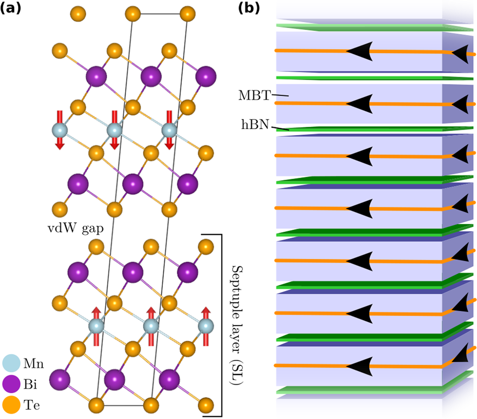
MBT appears as particularly promising due to, among other features, its van der Waals nature. Now a team of researchers proposes 1 a novel MBT-based high Chern number material: multilayers of MnBi2Te4/hBN.
The new design is a multilayer van der Waals heterostructure, in which thin MBT Chern insulator films are stacked on top of each other, interlayed by hexagonal boron nitride (hBN) monolayers that decouple and insulate them from one another. As an inert wideband gap insulator, hBN is an ideal material for such a decoupling, widely used in van der Waals heterostructure devices as an encapsulating layer or substrate for the stacked 2D materials.
Using state-of-the-art density functional theory and tight-binding calculations, the researchers show that the weak van der Waals bonding between MBT and hBN essentially preserves the C = 1 Chern insulator state in the individual MBT layers. Stacking n MBT films with C = 1 interlayed by (n − 1) hBN monolayers gives rise to a C = n state, with n as large as allowed by the van der Waals heterostructures growth technology.
This design approach allows a wide-range tuning of the Chern number, its upper limit being restricted only by the van der Waals heterostructures growth technology, making such multilayers interesting for future fundamental research and efficient interconnect technologies based on highChern number materials.
Author: César Tomé López is a science writer and the editor of Mapping Ignorance
Disclaimer: Parts of this article may have been copied verbatim or almost verbatim from the referenced research paper/s.
References
- Bosnar, M., Vyazovskaya, A.Y., Petrov, E.K., Chulkov, E.V., & Otrokov, M. M. (2023) High Chern number van der Waals magnetic topological multilayers MnBi2Te4/hBN. npj 2D Mater Appl doi: 10.1038/s41699-023-00396-y ↩