Real space geometry of aperiodic tilings as control knob for quantum physics
Real space geometry of aperiodic tilings as control knob for quantum physics
When we study solid-state physics, we usually begin with crystals. In a crystal, atoms repeat in a strict and regular pattern, much like tiles on a bathroom floor. Because every small region looks the same as every other, electrons move through a predictable landscape. This repeating order is the reason we can explain electricity, magnetism, and superconductivity using relatively simple ideas about waves and energy bands.
Not all solids follow this neat rule. There exists another class of structures called aperiodic tilings. These patterns are ordered, but they never repeat. No matter how far you zoom out, you will not find a unit cell that tiles the plane again and again. Quasicrystals are the most famous physical example of this idea. Their unusual order leads to electronic states that are neither fully localized nor fully spread out, and to symmetries that ordinary crystals cannot have.
Now, a team of researchers explores 1 a new kind of aperiodic tiling and shows that its geometry can be used as a control knob for quantum physics. The key point is that the pattern does not come in just one rigid form. Instead, it belongs to a whole family of related shapes that can be smoothly deformed into one another without ever becoming periodic. By changing the shape slightly, the entire tiling changes with it, while keeping its nonrepeating character. This single geometric change turns out to have a deep effect on how electrons behave.
The einstein family of aperiodic tilings
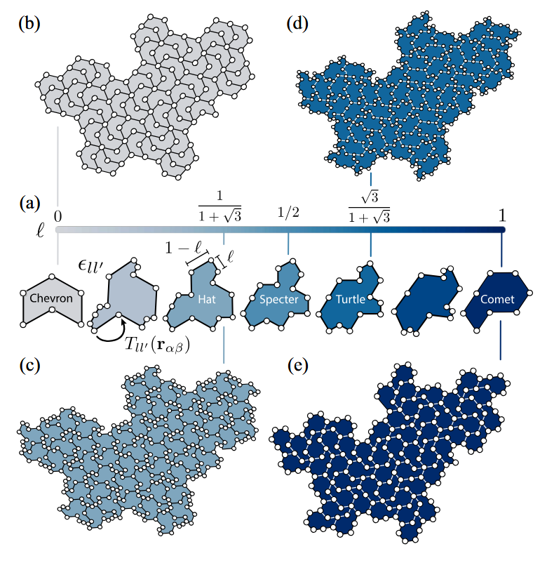
The story begins with a mathematical puzzle that stood for decades. Mathematicians searched for what they called an “einstein” tile, from the German words meaning “one stone”. The goal was to find a single shape that could cover a flat surface completely, but only in a nonrepeating way. In 2023, such a shape was finally discovered. It became known as the Hat tile, a simple polygon that forces aperiodic order wherever it is used.
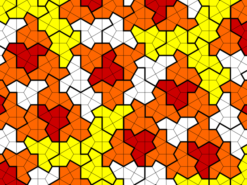
What makes the Hat especially interesting for physics is that it is not alone. It is part of a family of shapes that can be continuously stretched or compressed while keeping the same aperiodic structure. Physicists realized that this family could be used as a model playground for electrons. One can imagine placing an atom or an electronic site at every corner of the tiles and allowing electrons to hop from one site to another. When the tile shape is changed, the distances and angles between sites change too. This directly modifies how electrons move through the system.
In quantum mechanics, an electron is described by a wave function. Its behavior is governed not only by energy, but also by geometry. There is a mathematical object that captures this connection, often called the quantum geometric tensor. It contains two important pieces of information. One part describes how distances between quantum states are measured. This is known as the quantum metric and it tells us how spread out or compact an electron’s wave function is. The other part describes a kind of curvature in the space of quantum states. This curvature is linked to topological effects, which are responsible for special conducting states at the edges of materials.
In an ordinary crystal, these properties are largely fixed by symmetry. Once the lattice is chosen, the quantum geometry is mostly locked in. In the Hat family of tilings, something very different happens. Because the geometry can be tuned continuously, the quantum metric can also be tuned. By changing the tile shape, the researchers found that they could make the electron wave functions more localized or more extended. This is not just a mathematical curiosity. The quantum metric plays a role in how easily electrons can form supercurrents and how strongly they respond to light. In principle, adjusting geometry alone could help design materials with better superconducting properties or with tailored optical responses.
The topological part
The most striking effect appears in the topological part of the story. For certain shapes in the Hat family, the electronic system enters a topological phase. In such a phase, the interior of the material becomes insulating, while its edges host special states where electrons can move without resistance. These edge states are protected by global properties of the wave functions and cannot be easily destroyed by small imperfections.
What is remarkable here is that the transition into this topological phase is driven purely by geometry. By smoothly deforming the tiles, the system can be pushed from an ordinary insulating state into a topological one. Even more surprising, this topological behavior survives in the presence of disorder. Random imperfections, which usually disrupt delicate quantum effects, do not easily destroy the edge states in this aperiodic system. In some cases, disorder can even help create a topological phase. The nonrepeating geometry gives an additional layer of robustness that is not available in simple crystals.
Real space geometry as an active tool
This result changes how we think about material design. Traditionally, new electronic phases are sought by changing chemical composition or applying strong magnetic fields. Here, the main ingredient is real space geometry. The arrangement of sites alone, controlled by the shape of a tile, determines whether the system is trivial or topological and how its quantum states are distributed in space.
Of course, no natural metal is built from Hat tiles. The importance of this work lies in synthetic materials. Modern experiments can create artificial lattices using light, sound, or trapped atoms. Photonic systems guide light between resonators. Acoustic metamaterials guide sound waves. Cold atoms can be arranged with lasers into almost any pattern we choose. In these platforms, geometry is a design choice rather than a fixed constraint. One could draw an aperiodic tiling on a computer, build it in the laboratory, and then tune its quantum properties by changing a single geometric parameter.
Geometry is no longer just a backdrop for quantum physics. It becomes an active tool. By mastering the structure of a single nonrepeating tile and its deformations, physicists gain a new way to write quantum behavior directly into space. Instead of asking what a given material does, we can ask what pattern we should build to make electrons behave in a desired way. The humble act of tiling a plane, once a purely mathematical game, now opens a path toward designing future quantum materials.
Author: César Tomé López is a science writer and the editor of Mapping Ignorance
Disclaimer: Parts of this article may have been copied verbatim or almost verbatim from the referenced research paper/s.
References
- H. R. Carrasco, J. Schirmann, A. Mordret, and A. G. Grushin (2025) Family of aperiodic tilings with tunable quantum geometric tensor Phys. Rev. Lett. doi: 10.1103/dzqm-9kwj ↩
1 comment
An interesting read!
This quantum geometry is hiding many treasures it seems.
The tilings are all connected even though they are different ?