Electronic engineering of quantum dot arrays
Electronic engineering of quantum dot arrays
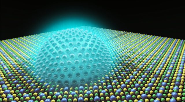
A quantum dot is a nanometric crystalline structure of semiconductor materials. In a quatum dot electrons are confined in a region of space, thus creating a well defined structure of energy levels that depends very much on the size and shape of the quantum dot. This structure resembles that of atoms, that is why sometimes quantum dots are also called artificial atoms.
Quantum dots aggregate to form QD-solids, suitable for many technological applications. The final properties of these solids depend on how the constituent quantum dots interact. Real QD-solids exhibit significant structural variations and the control of the potential barriers between neighbouring quantum dots is essential to tune the interaction between the existing units and engineer the two-dimensional electron gases (2DEG) present at the surface.
Self-assembled two-dimensional nanoporous networks are periodic extensions of quantum corrals that induce the confinement of scattered surface 2DEG electrons inside its nanocavities. Such regular nanostructures can be conceived as quantum dot arrays, where the surface adsorbed molecules change the local surface potential landscape. The confining barriers are characterized by a certain width and amplitude that affect the coupling degree of the neighbouring quantum dots.
Now, an international team of researchers, which includes members from CFM, UPV-EHU and DIPC, show 1 that precise engineering of the barrier width can be experimentally achieved on surfaces by a single atom substitution in a compound, which in turn tunes the confinement properties through the degree of quantum dot intercoupling.
Electronic engineering of 2DEGs can be achieved by tuning the molecular building blocks, thereby altering the quantum dot dimensions, the barrier amplitude and/or the barrier width. Moreover, changing the molecular compounds may also modify their interaction with the substrate, consequently altering the quantum dot electron confinement strength.

The researchers investigate two haloaromatic compounds that differ just in a single atom in their structure. Two different hexagonal molecular networks on a Ag(111) substrate are self-assembled that show single-molecular and double-molecular separation between their identical pores. The communication between neighbouring quantum dots is observed and evaluated following the 2DEG modification through a combination of scanning tunnelling microscopy/spectroscopy (STM/STS), angle resolved photoemission spectroscopy (ARPES) and extended model calculations.
The two molecules employed are 3,9-dibromodinaphtho[2,3-b:2′,3′-d]thiophene (Br-DNT) and [3,9-dibromodinaphtho[2,3-b:2′,3′-d] furan (Br-DNF). Structurally, arrays built from them can be conceived as extended model systems to investigate the 2DEG confinement and interpore coupling, as they feature identical quantum dots separated by different wall widths, namely, Br-DNT is single-walled (SW) whereas Br-DNF is double-walled (DW) (Figure 1).
These organic nanoporous networks are generated on bulk and thin Ag films alike by substitution of a single atom in the precursor molecule, reminiscent of a butterfly effect. The extended and periodic nature of these arrays provides access to their distinct band structures, which are directly compared with their local density of states and merged through calculations. Such complementary experimental and theoretical synergy provides complete fundamental insight into the nature of quantum dot intercoupling processes.
Even though substrate contributions cannot be discarded, the results clearly suggest that the reduction of the quantum dot coupling (from SW to DW) is associated with a flattening of the band dispersion and an increase of the effective mass.
This work not only complements the toolbox for tuning surface electronic properties, which started in the 90’s with the quantum corrals, but it is also prone to help in deriving clear conceptual ideas on quantum dot coupling, which is an essential parameter for next-generation technologies.
Author: César Tomé López is a science writer and the editor of Mapping Ignorance.
References
- Ignacio Piquero-Zulaica, Jorge Lobo-Checa, Ali Sadeghi, Zakaria M. Abd El-Fattah, Chikahiko Mitsui, Toshihiro Okamoto, Rémy Pawlak, Tobias Meier, Andrés Arnau, J. Enrique Ortega, Jun Takeya, Stefan Goedecker, Ernst Meyer & Shigeki Kawai (2017) Precise engineering of quantum dot array coupling through their barrier widths Nature Communications doi: 10.1038/s41467-017-00872-2 ↩