The intertwined nature of electronic waves in 2D TiSe2 crystals
The intertwined nature of electronic waves in 2D TiSe2 crystals
When we peel a crystal down to its very last layer, the physics governing its behavior undergoes a radical shift. This transition from the bulk (three-dimensional) to the two-dimensional limit is where some of the most exotic phenomena in condensed matter physics emerge. Among these, Titanium Diselenide, or TiSe₂, has long fascinated researchers because of its ability to undergo a phase transition into what we call a charge density wave (CDW). In this state, the electrons do not remain uniformly distributed across the crystal lattice, but instead reorganize themselves into a standing wave of charge.
To understand a charge density wave, imagine a crowded ballroom where people are standing in a rigid, repeating grid. If the individuals suddenly decide to shift their positions so that some areas become more crowded and others more sparse—creating a new periodic pattern overlaid on the original grid—they have formed a density wave. In TiSe₂, this happens because the electrons and the crystal lattice are deeply coupled. When the temperature drops, the electrons find it more “comfortable” to settle into this rippled pattern, which in turn causes the atoms to shift slightly from their original positions.
In the bulk (multilayer) version of this material, the CDW pattern is perfectly commensurate, meaning the electronic wave repeats exactly every two atoms (a 2×2 pattern) in all directions. Earlier studies have shown that even in a single atomic layer, TiSe₂ can form a robust CDW, often with a transition temperature higher than in the bulk—around 230 K versus about 200 K in the bulk. This is counterintuitive, because reducing a material to a single layer usually makes ordered states more fragile due to stronger thermal fluctuations. Here, however, the reduction in dimensionality seems to lock the electrons into their new pattern more effectively.
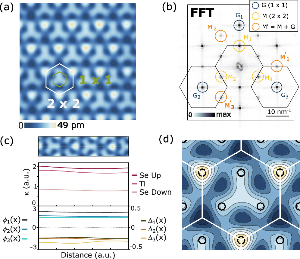
A recent study 1 explored this phenomenon in ultraclean single-layer TiSe₂—specifically, slightly doped monolayers grown on a substrate that introduces a small amount of extra electrons. Using high-resolution Scanning Tunneling Microscopy (STM), the researchers directly visualized the electronic waves and discovered a surprisingly intricate and robust state. While the pattern resembles a 2×2 grid at first glance, it is not perfectly commensurate. Instead, the electronic waves form a near-commensurate state, with a longer wavelength (around 20 nm) and subtle variations across the surface.
The most striking finding is that these waves are “intertwined”: the CDW consists of coupled components of different symmetries that form an ordered network of unidirectional domain walls—almost like domain boundaries where the wave pattern shifts or flips in a coordinated way. This creates regions that are locally commensurate, separated by these ordered defects rather than random slips. The result is a delicate balance where the electrons are almost, but not quite, perfectly in sync with the atoms. This near-commensuration is significant because it makes the electronic state highly tunable—even small changes, such as slight additional doping or applied strain, could dramatically alter the material’s properties.
This “intertwined” nature of the charge density waves is particularly exciting because it mirrors the complexity seen in high-temperature superconductors. In those materials, different types of electronic orders—like magnetism and charge waves—often compete or cooperate to enable zero-resistance electricity. By studying TiSe₂ in its simplest, two-dimensional (and slightly doped) form, we gain a cleaner laboratory to understand how these collective electronic behaviors emerge and how we might eventually harness them for new types of quantum electronics. The transition from a perfect bulk crystal to this near-commensurate, intertwined single layer proves that in the world of advanced materials, less is often much, much more.
Author: César Tomé López is a science writer and the editor of Mapping Ignorance
Disclaimer: Parts of this article may have been copied verbatim or almost verbatim from the referenced research paper/s.
References
- W. Wan, M. N. Gastiasoro, D. Munoz-Segovia, P. Dreher, M. M. Ugeda, and F. de Juan (2026) Near-commensuration from intertwined charge density waves in single-layer TiSe₂ Nano Lett. 26, 816 doi: 10.1021/acs.nanolett.5c05317 ↩