Visualizing obstructed atomic phases in 2D materials
Visualizing obstructed atomic phases in 2D materials
In the world of quantum materials, some of the most important discoveries come not from finding new particles, but from learning to see familiar electrons in a new way. A striking example comes from a single layer of niobium diselenide, a crystal just one layer thick, where researchers have now directly mapped a hidden pattern in the way electrons occupy space inside the material. Their result confirms a long-standing prediction in condensed matter physics: electrons can form a band that looks perfectly ordinary in its energy structure, yet still be arranged in a deeply nontrivial geometric way inside the crystal.
An obstructed atomic phase
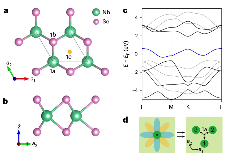
In a crystal, at the atomic scale, atoms sit in a repeating lattice, like the repeating tiles of a floor. In most introductory models, electrons associated with a given band are imagined as being centered on the atoms themselves. Their “home base,” so to speak, coincides with the positions of the nuclei. But quantum mechanics allows something subtler. The electronic charge can instead be centered in the empty spaces between atoms, while still respecting the symmetry of the crystal and remaining tightly localized. This is the essence of what physicists call an obstructed atomic phase. It is “atomic” because the electrons remain localized, but “obstructed” because their centers cannot be smoothly moved back onto the atoms without changing the quantum structure of the band.
A new methodology
For years, this idea was theoretically elegant but experimentally frustrating. The challenge was not proving that such bands could exist, but actually measuring where the electronic weight lives in a real material. The breakthrough here 1 came from combining scanning tunnelling microscopy with first-principles electronic structure calculations. Scanning tunnelling microscopy can measure how electronic states are distributed across a surface with atomic resolution, effectively turning the crystal into a quantum landscape map. By carefully analyzing these real-space spectroscopic images, the researchers reconstructed how different atomic orbitals in the material are correlated with one another. This allowed them to infer the true spatial center of the electronic band that crosses the Fermi level, the energy frontier most relevant for electrical behavior.
In the spaces
What they found is conceptually beautiful. In monolayer niobium diselenide, the relevant electronic band behaves as if its charge center sits not on a niobium or selenium atom, but on an empty symmetry point inside the unit cell. In other words, the most natural description of the electrons places them in the spaces defined by the crystal, rather than on the atoms that build it. This may sound almost philosophical, but it has real physical meaning. The geometry of where electrons are centered shapes how they respond to defects, edges, strain, and even how they may participate in more exotic collective states.
It is as if the electrons have quietly claimed the open spaces of the crystal as their true home.
The broader significance goes beyond one compound. Niobium diselenide belongs to the family of transition metal dichalcogenides, layered materials that have become central to modern quantum materials research because they can host superconductivity, charge ordering, and unusual topological effects. By showing that one of their electronic bands has this obstructed structure, the work opens a new route for understanding how real-space geometry influences electronic phases in two dimensions. The same method should also apply to many other layered compounds where topology is encoded not in edge currents or magnetic responses, but in the quiet geometry of localized electrons.
A band can be localized, compact, and seemingly simple, yet still hide a subtle internal geometry that changes how we classify the material. What makes this advance so exciting is not only that it verifies a beautiful theoretical concept, but that it gives experimentalists a practical way to visualize this hidden electronic geometry directly in real space.
Author: César Tomé López is a science writer and the editor of Mapping Ignorance
Disclaimer: Parts of this article may have been copied verbatim or almost verbatim from the referenced research paper/s.
References
- Dumitru Călugăru, Yi Jiang, Haojie Guo, Sandra Sajan, Yongsong Wang, Haoyu Hu, Jiabin Yu, B. Andrei Bernevig, Fernando de Juan, and Miguel M. Ugeda (2026) Observation of an obstructed atomic band in a transition metal dichalcogenide Nature Physics doi: 10.1038/s41567-026-03196-5 ↩